MESA+ HIGHLIGHTS 2022


PREFACE 1 NANOLAB 2 CENTRES OF EXPERTISE 3 HIGHLIGHTS PI’S 4

Dear MESA+ colleagues,
With only a few days left this year, the Christmas break is just around the corner. It is time to reflect on the past year, in which many results were achieved. As in last year, we want to look back at the highlights of the year with this digital magazine: an overview with highlights of the NanoLab, our centres of expertise and, of course, of our PIs.
On 1 April 2022, MESA+ took over the programme office of MinacNed and Nano4Society. By bringing both programme offices under one roof, in addition to the programme office of NanoLabNL, which we have been running for some years now, we will fortify the ecosystem and infrastructure in the field of nanotechnology in the Netherlands and work on solutions for major societal challenges. This way, we take a stronger (inter)national role and hope to increase our societal impact and economic value even more.

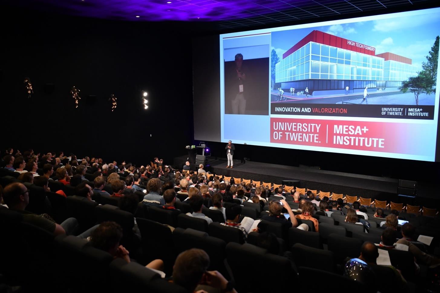
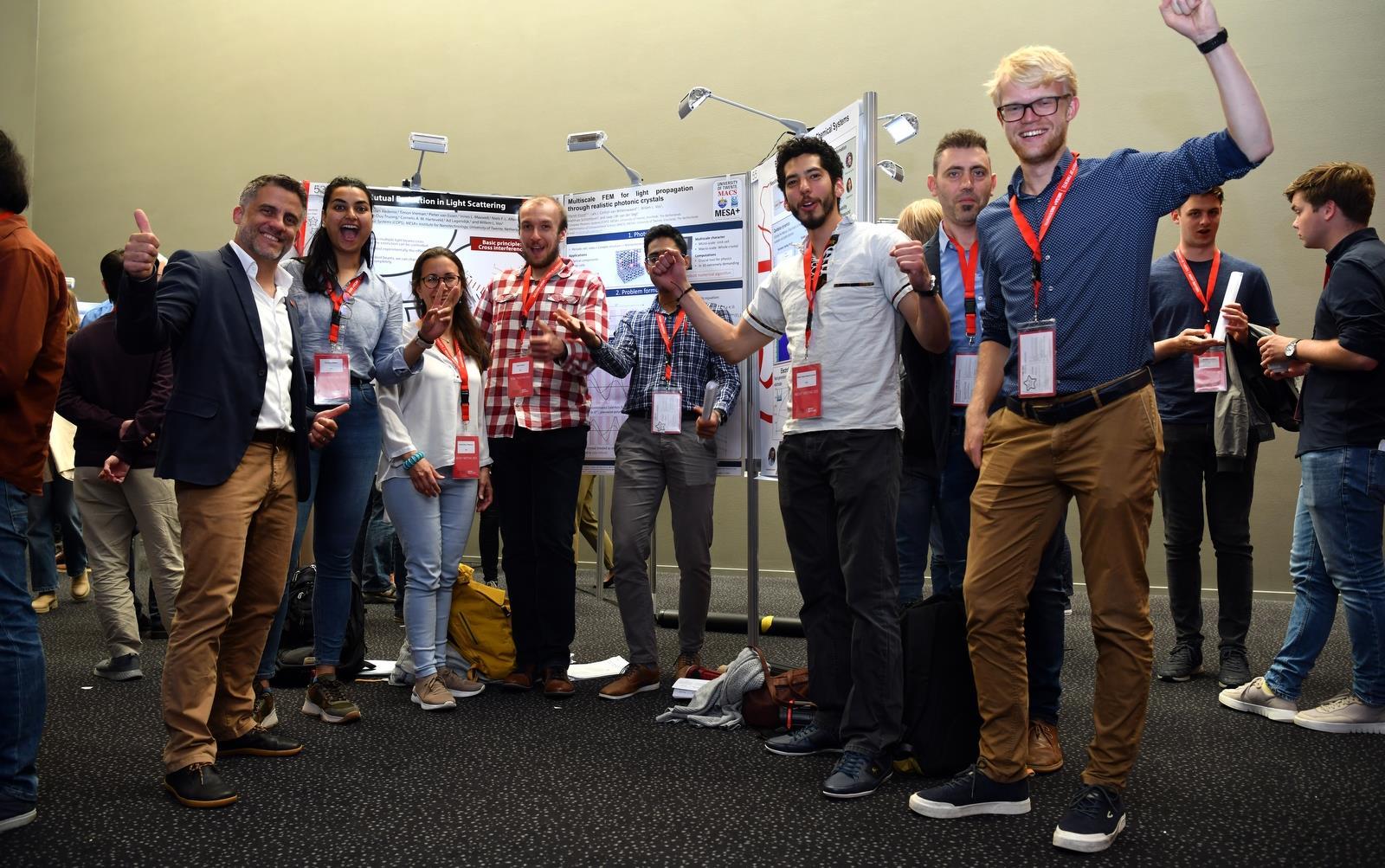
On 13 June 2022, we organised the MESA+ Meeting at Kinepolis in Enschede. After an online edition in 2020 and skipping a year in 2021, we enjoyed a day full of knowledge exchange, inspiration, networking, and meeting socially. We look back on a successful edition of this meeting and hope to see you again at the next MESA+ Meeting on: 25 September 2023 Save the date!
As we did last year, we put much time and energy into writing the National Growth Fund proposals. And we had success! For instance, phase two of Quantum Delta NL was approved this year, and 333 million was reserved for phase three. In this second phase, a further portion was also released for NanoLabNL, aiming to maintain and develop the Dutch national infrastructure in nanotechnology further. Within Quantum Delta NL, funds are also available for Nano4Society and MinacNed.
Recently, the PhotonDelta growth fund was also approved. Currently, discussions are ongoing with the ministry of economic affairs about the exact conditions under which funds will be allocated. The expected start date will be Q3 2023. The PhotonDelta growth fund aims primarily at increasing production capacity for integrated photonics and focusing on next-generation integrated photonics with a particular focus on hybrid integration. To achieve these goals, funds that are allocated are available for cleanroom equipment for higher TRL applications and research projects. These activities align well with our efforts to establish a High Tech Factory to allow for upscaling production of chip production.
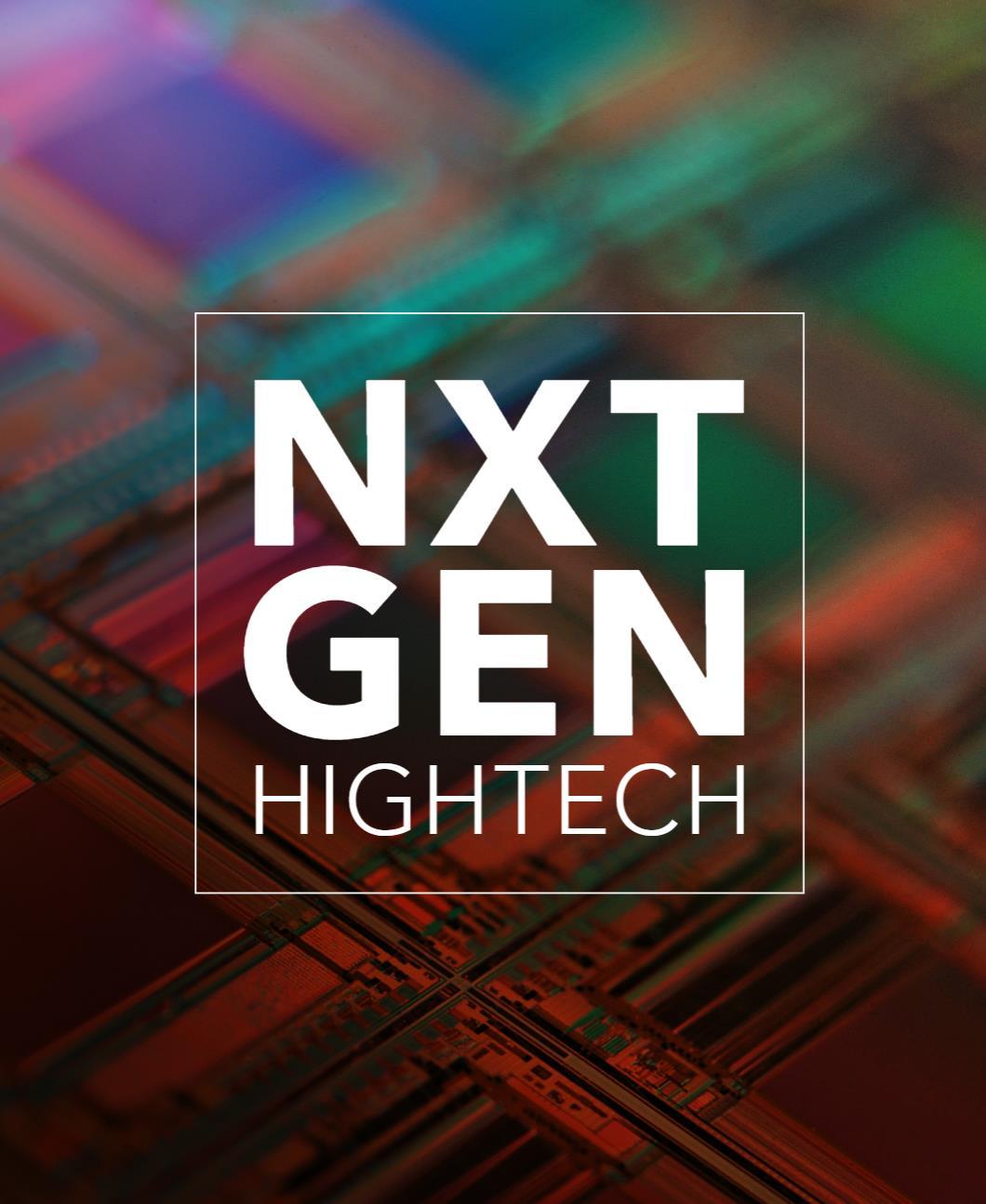
In addition to PhotonDelta and Quantum Delta NL, NXTGEN HIGHTECH was also approved. The program aims to start in Q1 2023 and focuses on the new generation of high-tech equipment for future generations. Over a seven-year period, the programme will invest ~€1 billion (of which approximately half will be from the National Growth Fund) in six key application areas for generations to come, i.e. 1) Clean energy, 2) Data communication via light, 3) Equipment for faster medicine development without animal testing, 4) Faster microchips, 5) Innovative production of light composite materials, and 6) Fast and precise robots in agriculture and horticulture. The aim is to make this Dutch high-tech equipment ecosystem a leader in Europe by 2040, with an ultimate contribution to GDP of ~€10 billion per year. The UT, and MESA+ specifically, is very well positioned within this NXTGEN HIGHTECH growth fund programme.
We
thank
been writing these proposals for the National Growth Fund ("nationale groeifondsen") for their time, energy, and enthusiasm. It is great that this was a successful joint effort. With the proposals approved in the first and second rounds and the proposals submitted for the third round, MESA+ has firmly positioned itself on all these fronts. These proposals will offer great opportunities for the near future.
want to
everyone who has
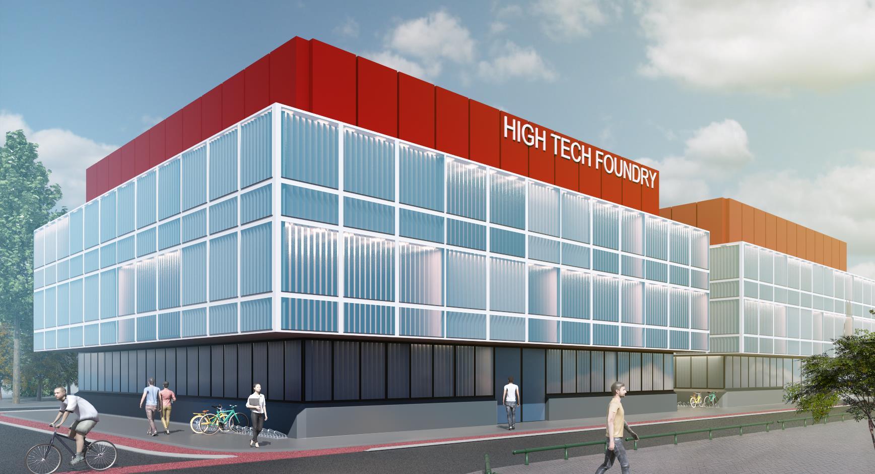
In the past decades, a variety of companies have spun out from MESA+. A number of these have always relied on the services of the MESA+ NanoLab for research and development as well as chip production. As many of these companies are maturing, we are seeing a steady increase in cleanroom use associated with commercial production. This is a success story but it also presents us and our ecosystem with the challenge that continued expansion of production capacity must be accommodated. The MESA+ NanoLab will not be able nor is established to fulfill this role. We have therefore initiated plans to expand our local ecosystem with a High Tech Foundry where commercial chip production can take place. Gradually, these ambitions have expanded to the initiative of the ChipTech Twente, where not only infrastructure for chip production but also chip design, talent development and research and development in heterogeneous integration are combined.
Chip Tech Twente is a joint effort of the key regional players in chip technology, a.o. MESA+, Kennispark, OostNL, Twenteboard, NovelT and numerous chip tech companies. MESA+ has taken the lead in establishing ChipTech Twente and will continue to do so. This initiative brings several key expertises of MESA+ together: Chip design, integrated photonics, microfluidics and quantum technology. Together with our state of the art infrastructure and our ambitious and realistic plan for establishing a high tech foundry, we have all ingredients available to position Twente as Europe’s gateway for innovative chip design and heterogeneous systems.
The MESA+ NanoLab will continue to be the center for academic research as well as a place where established and newly started companies can conduct research and development and pilot production with the possibility to obtain the services of the The High Tech Foundry for required production capacity.
MESA+ has various centres of expertise which provide PI’s with the opportunity to raise the profile of their research within and outside the University of Twente, as well as the tools for bottom-up organisation and management. MESA+ can offer support to enable centres to develop themselves, provided that the centres align with the heart of the research strategy of MESA+ and they have sufficient focus and mass. This year we started to evaluate the centres and support them to make them more impactful. Currently, the following MESA+ centres are operational:

We hope to offer a nice way of looking back on 2022 with this magazine, because it was a year in which great results were achieved, and we are proud of that! This magazine will offer everyone a stage to share their highlight of the year, so that we within the MESA+ family know what everyone has been working on and be able to show how much talent we accommodate. We look back on 2022 with pride and want to thank you all for your ongoing dedication, flexibility, and commitment!
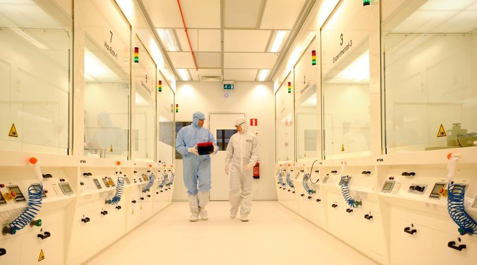
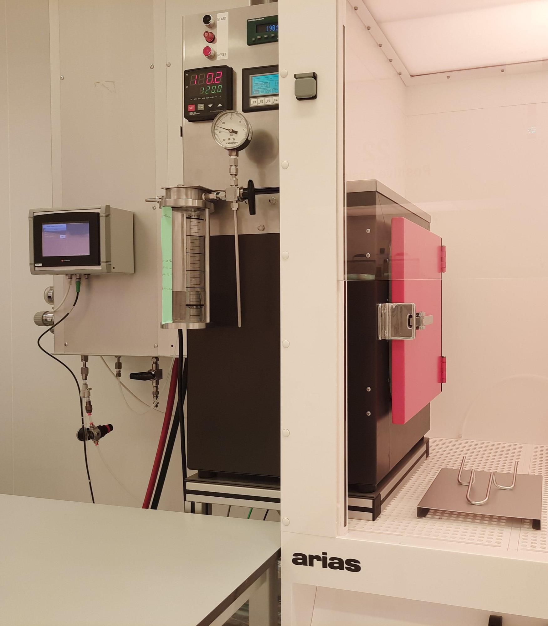
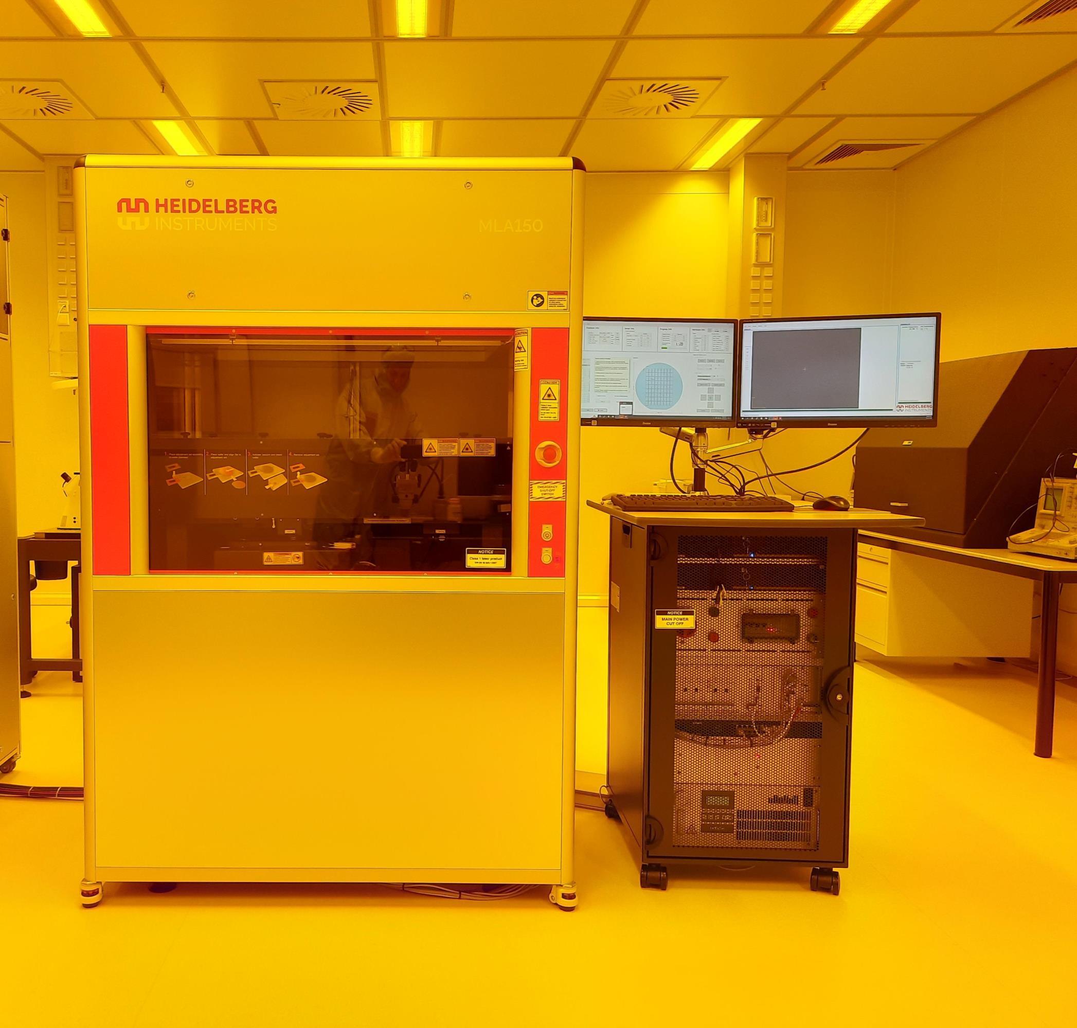
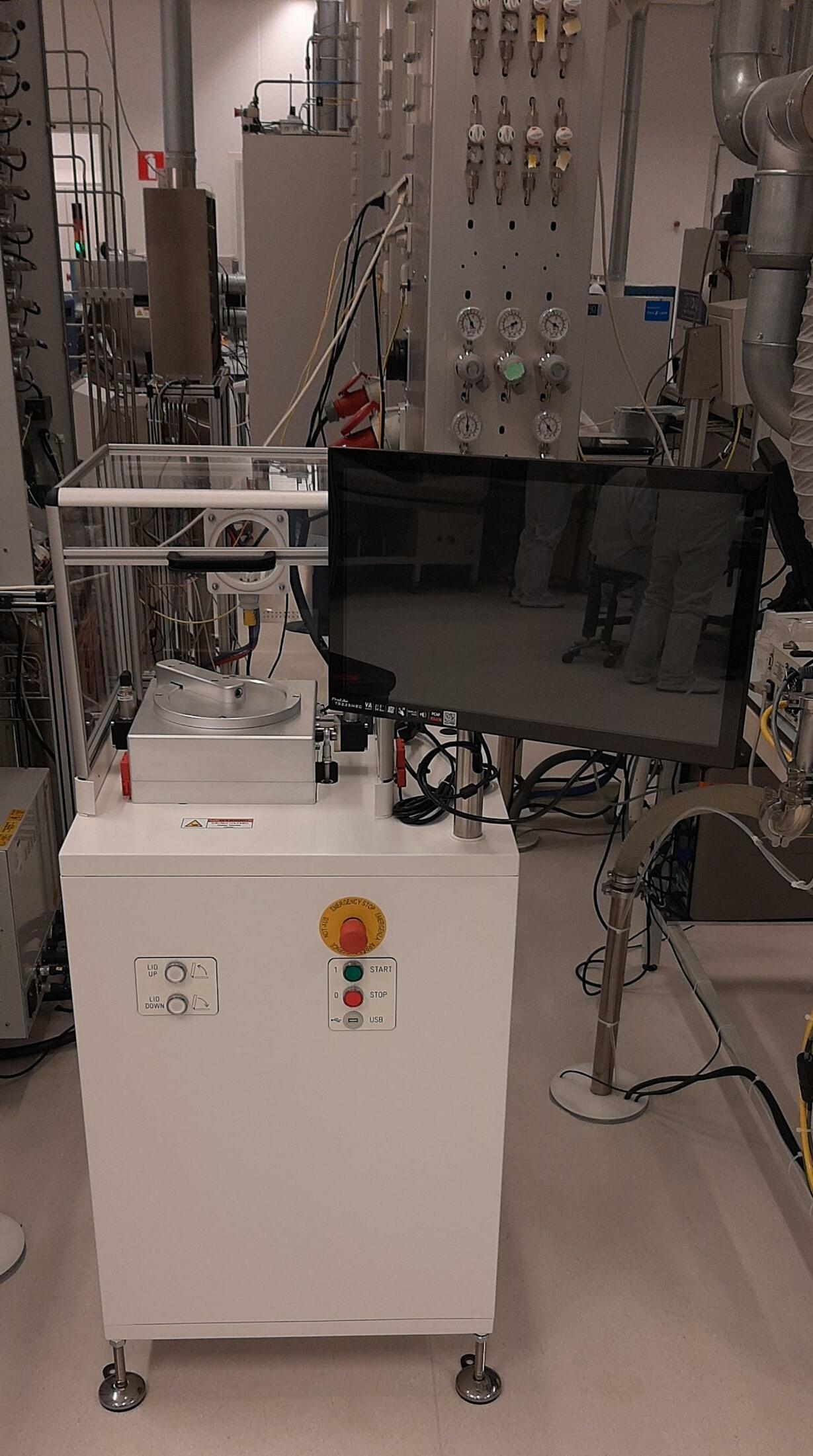
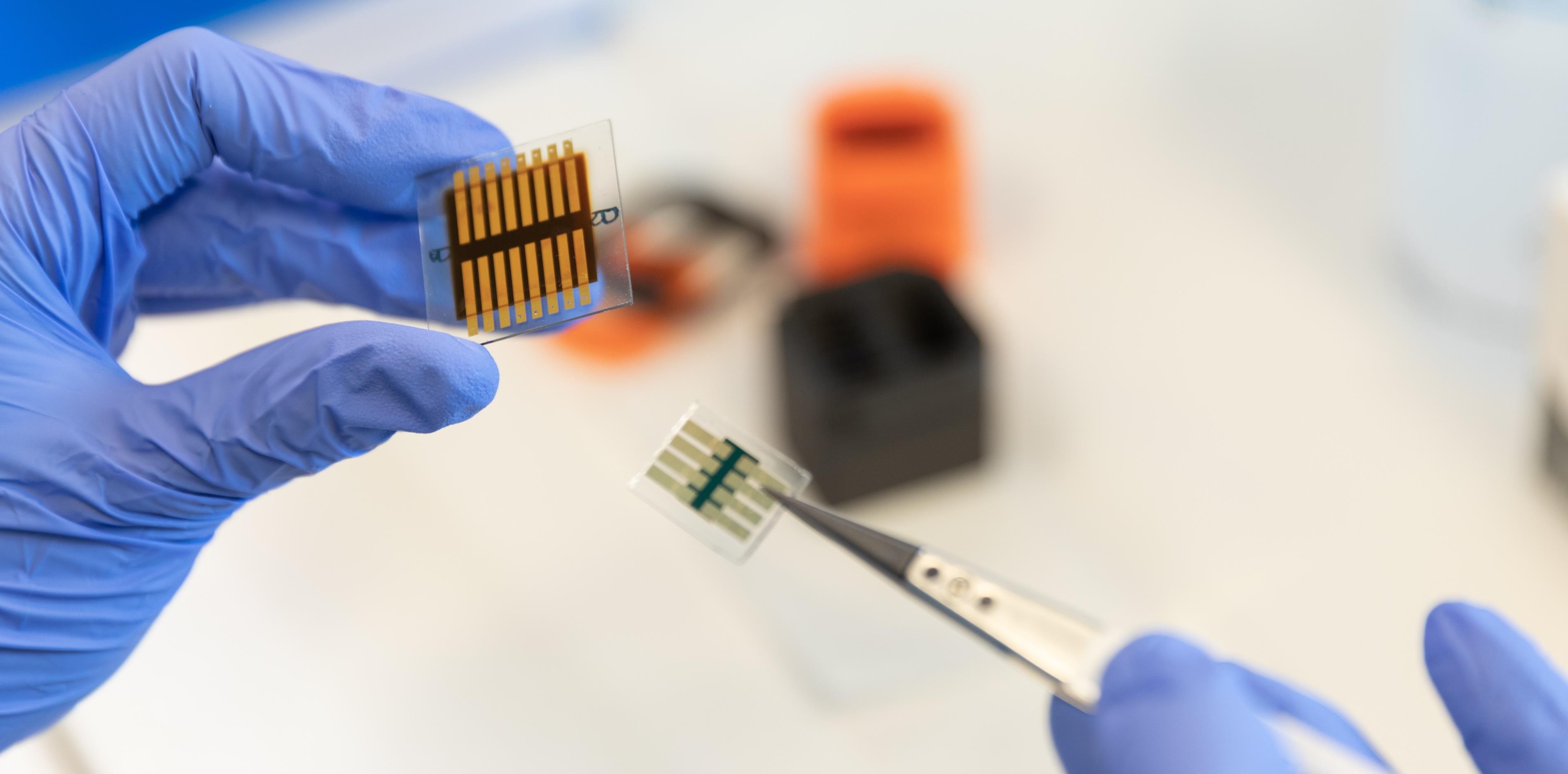
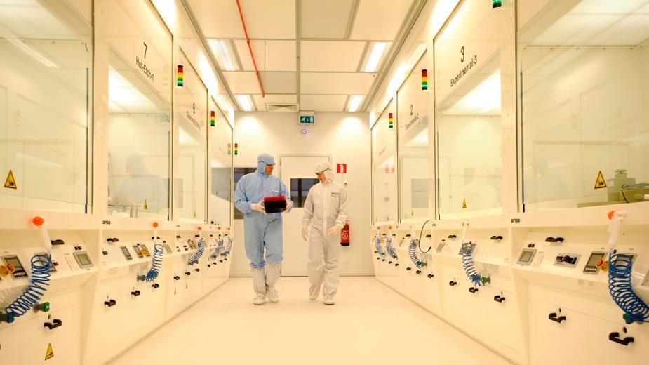
NanoLab's positioning is becoming increasingly stronger, both within and outside the UT. This is due to a motivated team working daily on the growth and further development of the NanoLab. On the following pages, you'll find an overview of two new facilities that have recently been installed.
The HMDS oven is an automated priming system for wafers. Up to two wafer boats of 25 wafers each can be processed in one run. The oven provides a fast and uniform priming of wafer surfaces with hexamethyldisilizane (HMDS) to improve the adhesion of photoresist.
The combination of vacuum, heat and N2 purge ensures a thorough dehydration before the deposition of HMDS.

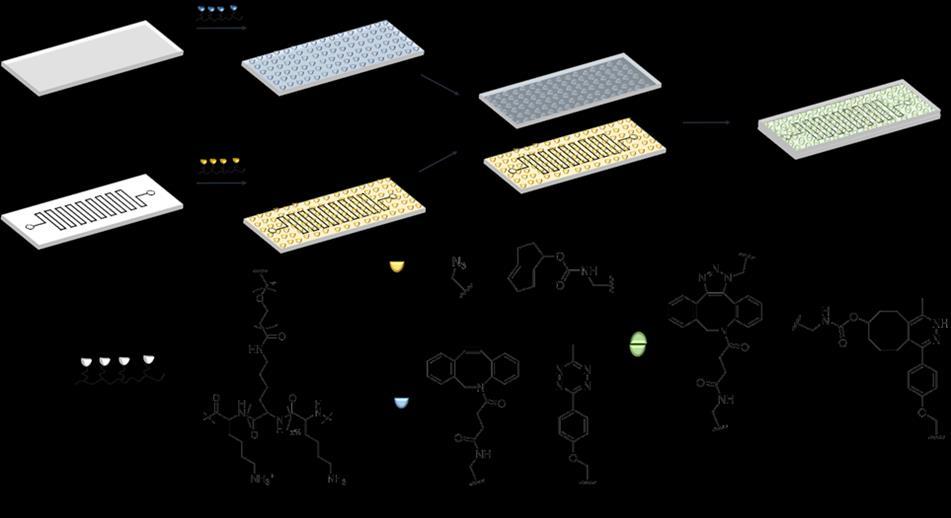
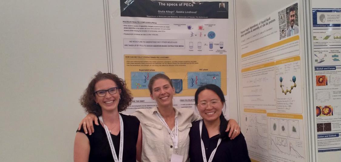
Enabling technology, innovation and collaboration for the next generation Organ-On-Chips
Further growth towards collaboration and impact with:
• 18 Publications in peer-reviewed literature
• Developing educational packages
• Design of M.Sc. course on Organ-on-Chip
• Pilot of Organ-on-Chip Summer School
• Hosting multiple workshops on Organ-on-Chip technologies

• Key involvement in (inter)national consortia funded by NWO and Europe
• New programme leadership: welcome Sanne de Wit!
Supported by www.utwente.nl/oocct


MESA+ coordinates these four strategic impulse programmes to empower strategic research

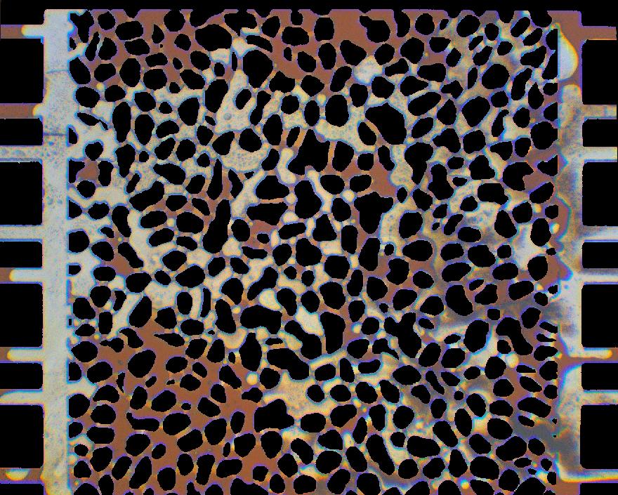
 Picture: Testing PLD-grown hybrid halide perovskites and transparent contacts in proof-of-concept Solar Cells PI: Monica Morales-Masis. M3 Lab @ IMS
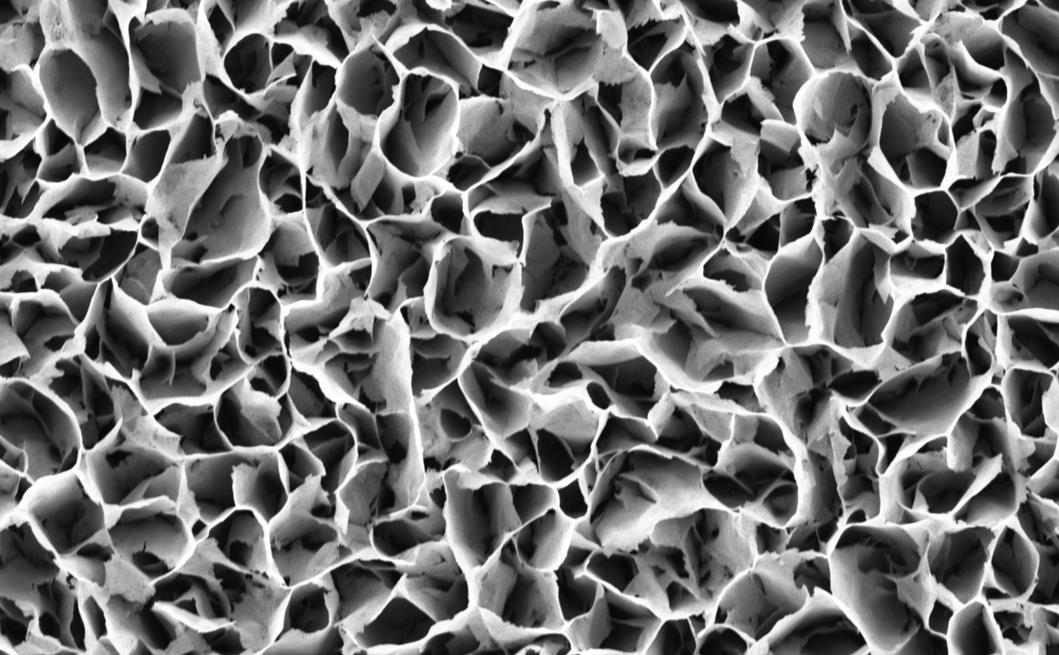
We mimicked carbonate rock in a microfluidic setup by functionalizing a dual-depth (2.5D) glass chip with calcite particles. Injecting salty water (from the left) displaces oil (brown) in an incomplete manner. Due to the hydraulic and capillary forces, a preferred flow path gets formed quickly. In some pores a layer of oil remains and gets bypassed by the flow. At longer times water droplets get formed inside the oil.
 Michel Duits, Physics of Complex Fluids

Microtechnology allows us to fabricate sensors with better specifications. This sensor is designed for real-time leaf-level air flow measurements to improve the microclimate around plants in greenhouses and vertical farms. We are currently working on the integration of sensors with electronics: a single chip that – in the future – translates any physical parameter from the real world into a digital signal.
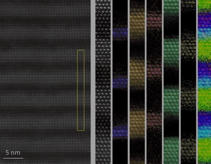
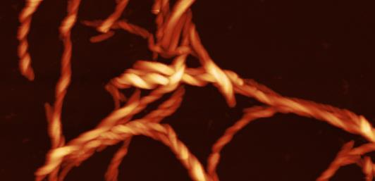
When a topological insulator is made ultrathin, the topological surfaces at the top and bottom of the film are predicted to hybridize, leaving only quantized edge state electronic transport. In order to pursue this effect, we developed ultrasmooth films of Bi2-xSbxTe3 by molecular beam epitaxy. The colors in the atomic force microscopy image show terraces with different integer numbers of unit cells.
Nanomaterials 12, 1791 (2022).
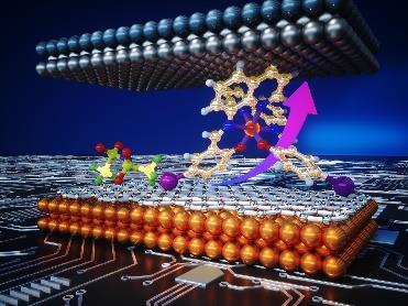 A. Nijhuis – Hybrid Materials for OptoElectronics
We are developing molecular hardware based on switches that are complementary to traditional electronic devices based on semi-conductors. We developed molecular device that can be re-configures in all Boolean logic-gates.
Adv. Mater. 2022, 22, 2270197.2270197
Other research interests include:
- Plasmonic tunnel junctions
- Neuromorphic devices
- (bio)molecular electronics
Christian- Additive manufacturing of inorganic materials with luminescent properties (RGB emission)
- Additive manufacturing of inorganic semiconductors (perovskites)
- Photo-induced processes at the mesoscale (photochemical reactions)
 J. Winczewski et al., Adv. Optical Mater. 2022, 2102758
Arturo Susarrey Arce & Mesoscale Chemical Systems
J. Winczewski et al., Adv. Optical Mater. 2022, 2102758
Arturo Susarrey Arce & Mesoscale Chemical Systems
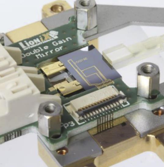
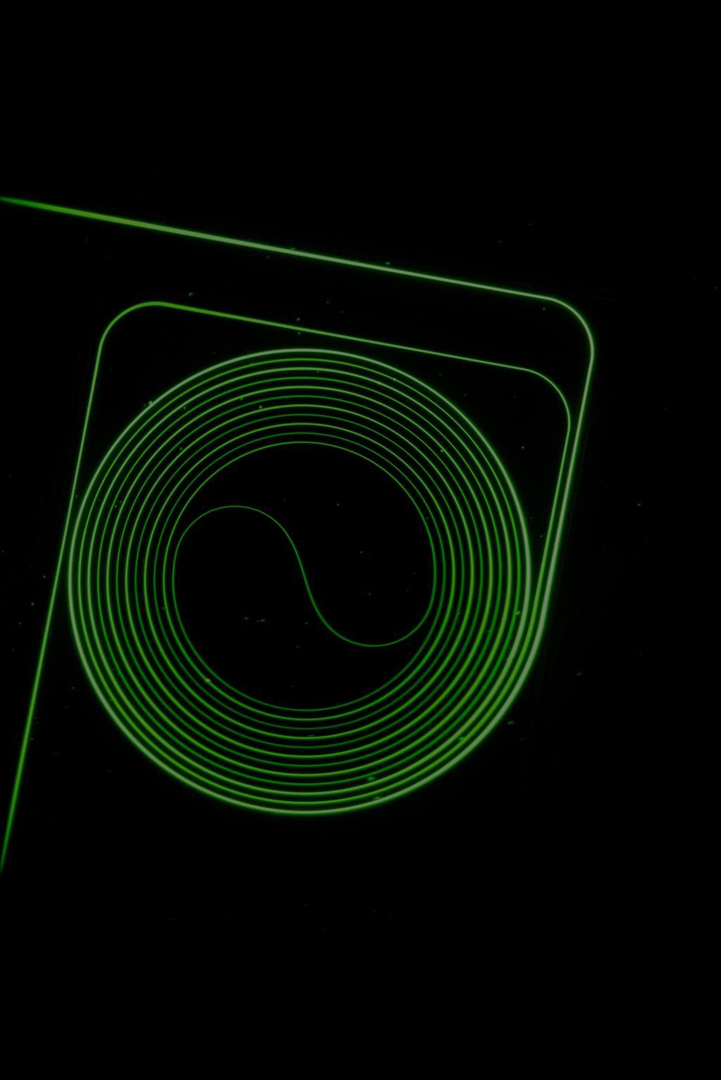
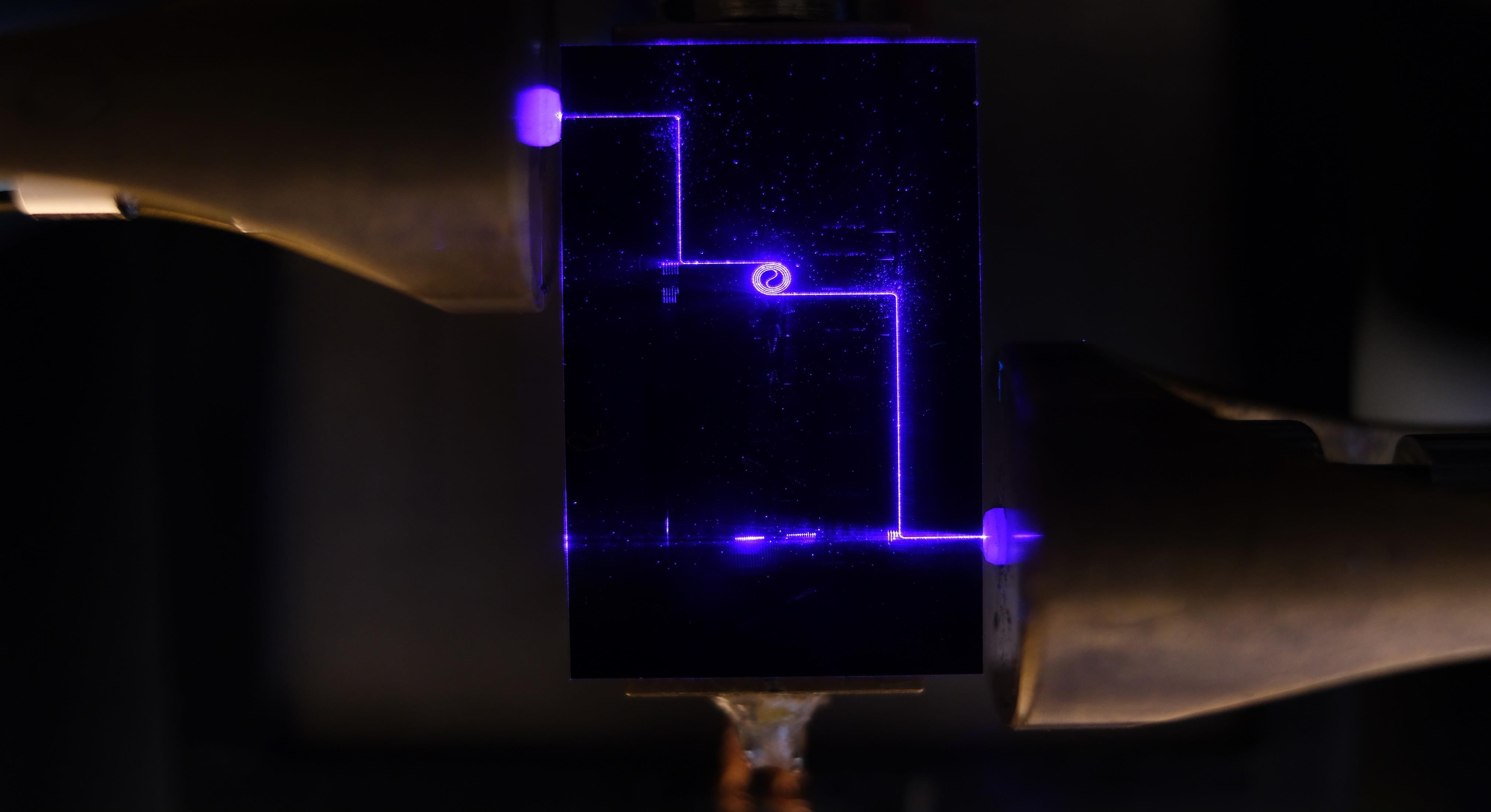
We measured the first stimulated Brillouin scattering signal in double-stripe silicon nitride waveguides. This opens the way to achieving Brillouin-based photonic circuits in a standard, low-loss silicon nitride platform.
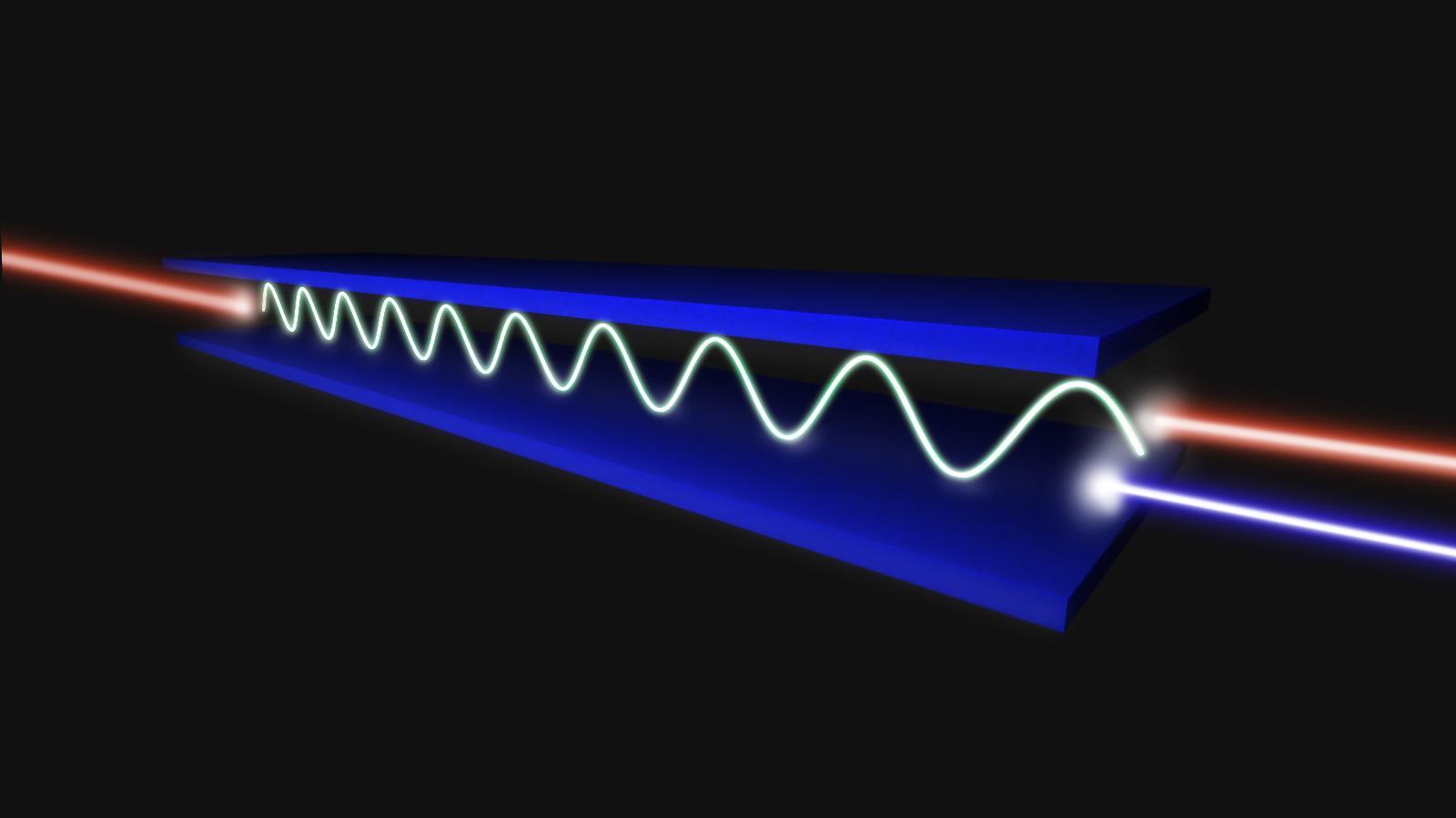
Botter et al., Sci. Adv. 8, eabq2196 (2022)
David Marpaung | Nonlinear Nanophotonics
.
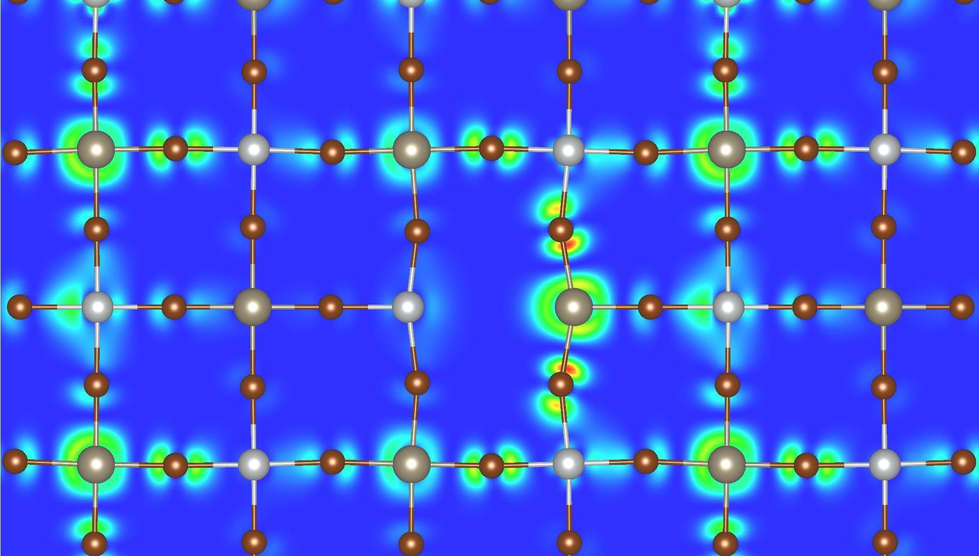
Theory predicts that the application of an electric field breaks the inversion symmetry in AB and BA stacked domains of twisted bilayer graphene. Here we show that the application of an electric field results in the formation of a two-dimensional (2D) network of 1D topologically protected conduction channels. We provide compelling experimental evidence that the electronic transport in these counter-propagating one-dimensional channels is dissipation less.
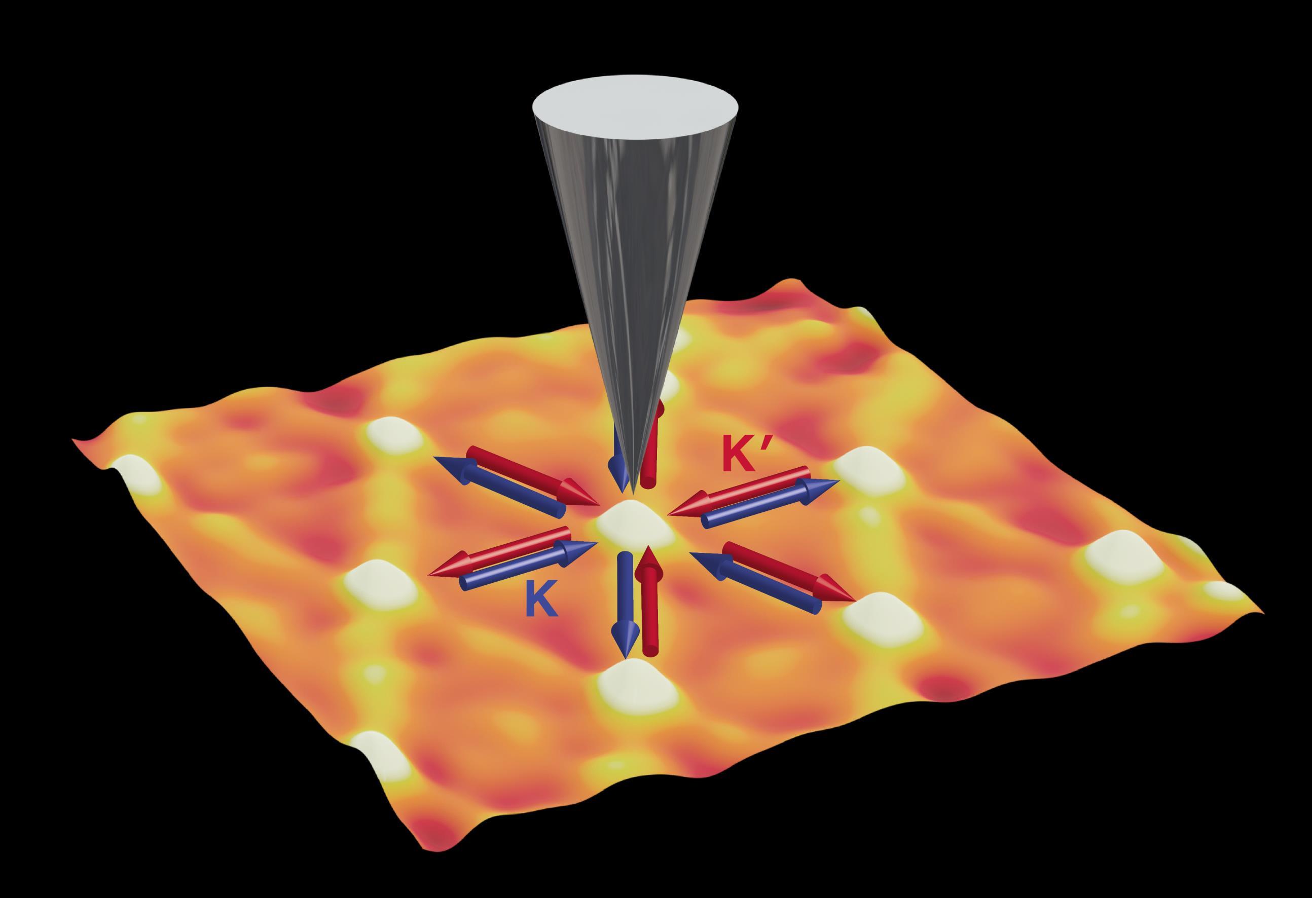
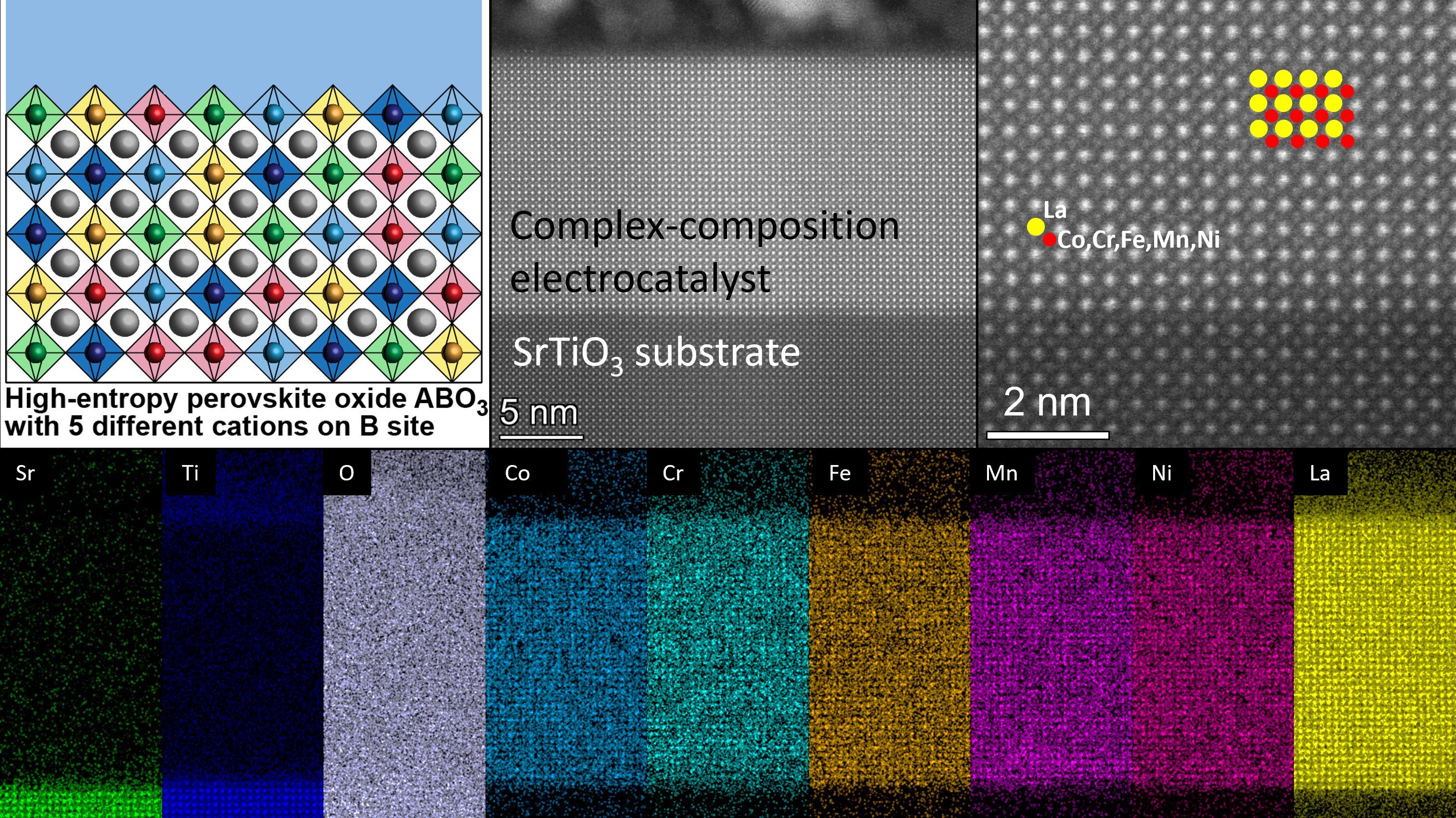
 Gertjan Koster - Physics of Inorganic Nanomaterials (IMS)
Binbin Chen, Nicolas Gauquelin, Nives Strkalj, Sizhao Huang, Ufuk Halisdemir, Minh Duc Nguyen, Daen Jannis, Martin F. Sarott, Felix Eltes, Stefan Abel, Matjaž Spreitzer, Manfred Fiebig, Morgan Trassin, Jean Fompeyrine, Johan Verbeeck, Mark Huijben, Guus Rijnders & Gertjan Koster , Nat. Comm. Jan. 2022
Gertjan Koster - Physics of Inorganic Nanomaterials (IMS)
Binbin Chen, Nicolas Gauquelin, Nives Strkalj, Sizhao Huang, Ufuk Halisdemir, Minh Duc Nguyen, Daen Jannis, Martin F. Sarott, Felix Eltes, Stefan Abel, Matjaž Spreitzer, Manfred Fiebig, Morgan Trassin, Jean Fompeyrine, Johan Verbeeck, Mark Huijben, Guus Rijnders & Gertjan Koster , Nat. Comm. Jan. 2022
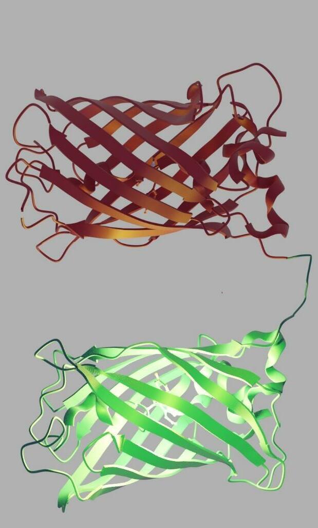
GFP only expressed in the parasite
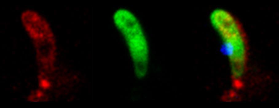
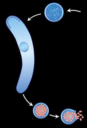
Malaria parasite in the ookinete stage
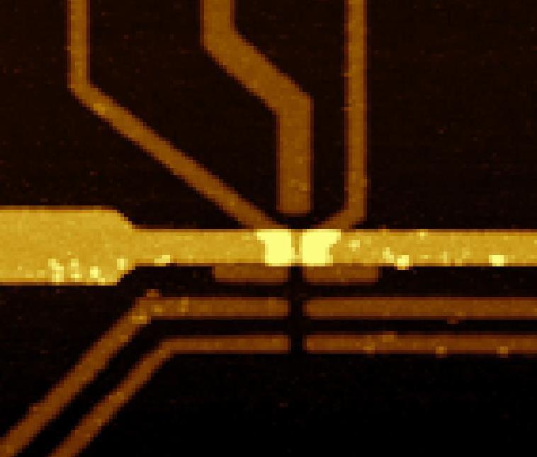
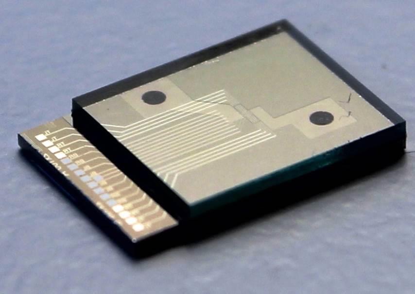
Serge G. Lemay, Bioelectronics

We introduced a framework for the fabrication of chip-based electrochemical nanogap sensors integrated with microfluidics. SU-8 aided adhesive bonding of silicon and glass wafers is used to implement parallel flow control. This permits wafer-scale production of monolithic structures with simple electrical and fluidic interconnects.
•
•

 Marko Sturm – Industrial Focus Group XUV Optics
One of the research activities of IDS group is adding unique features to atomic layer deposition (ALD) equipment, which are not readily available elsewhere. Our ALD reactors are equipped with a hot wire, which is a very local source of thermal energy. So, we develop and study Hot-Wire enhanced ALD (HWALD) processes. HWALD has several advantages over conventional plasma-enhanced deposition: it is cheaper and easier to implement, deposition chemistry can be simplified giving a better control of the process and film’s quality.
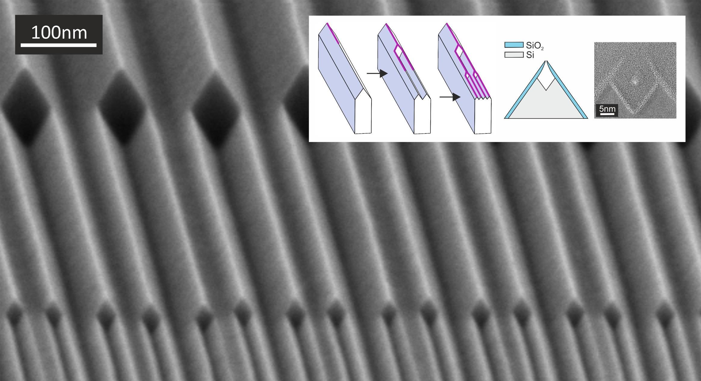
3D Integrated Nanosystems, MCS
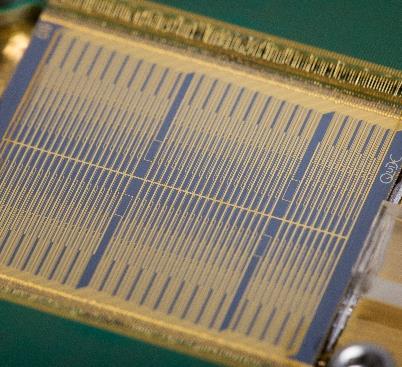
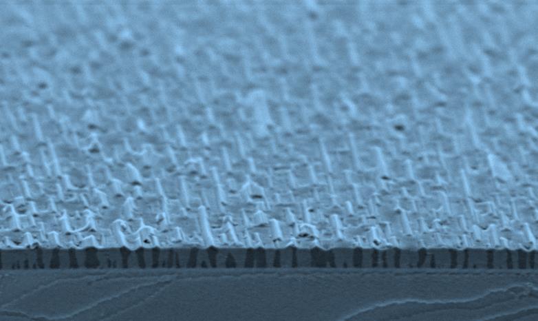
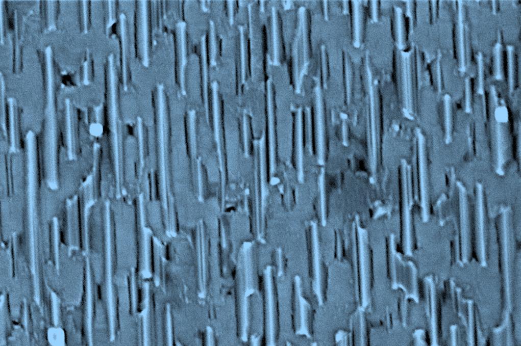
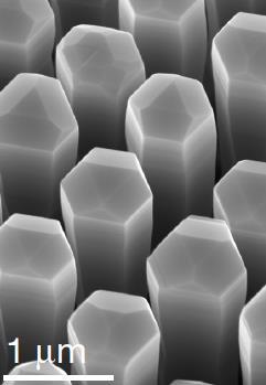
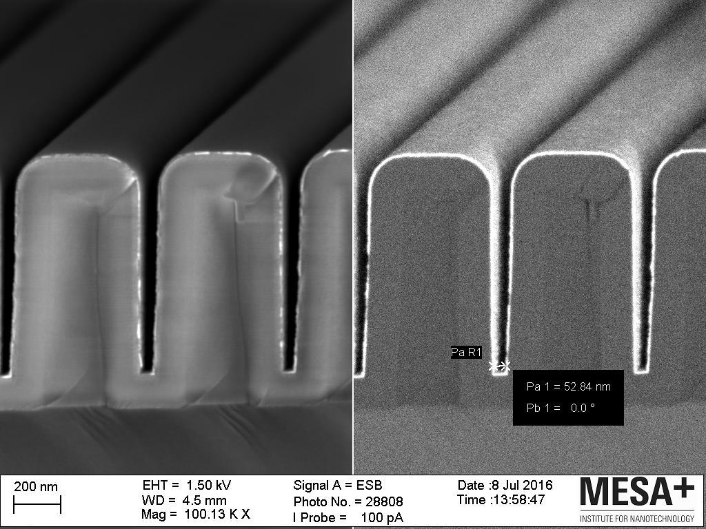
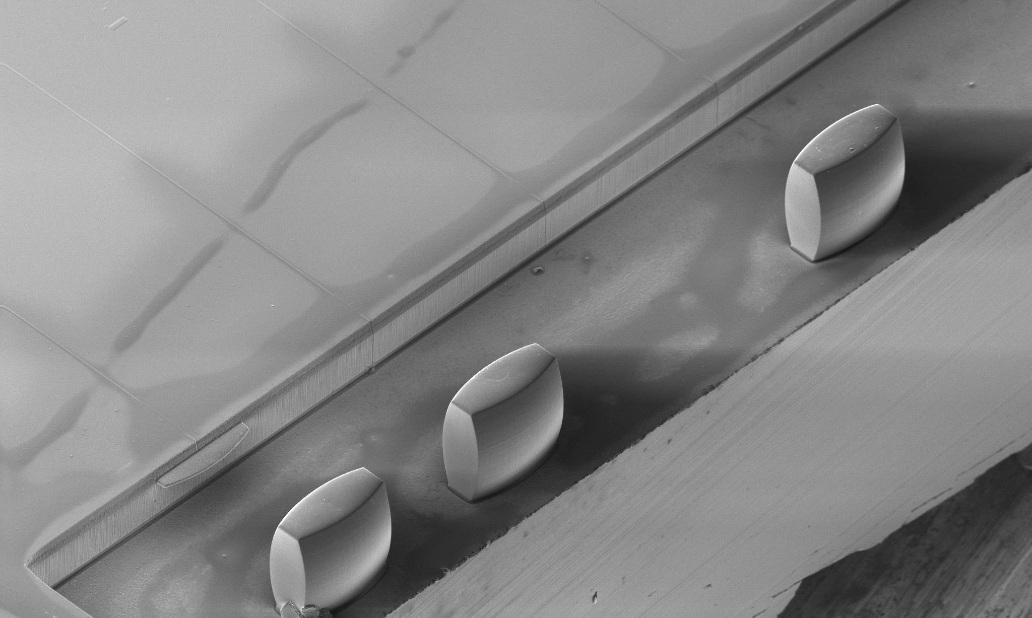
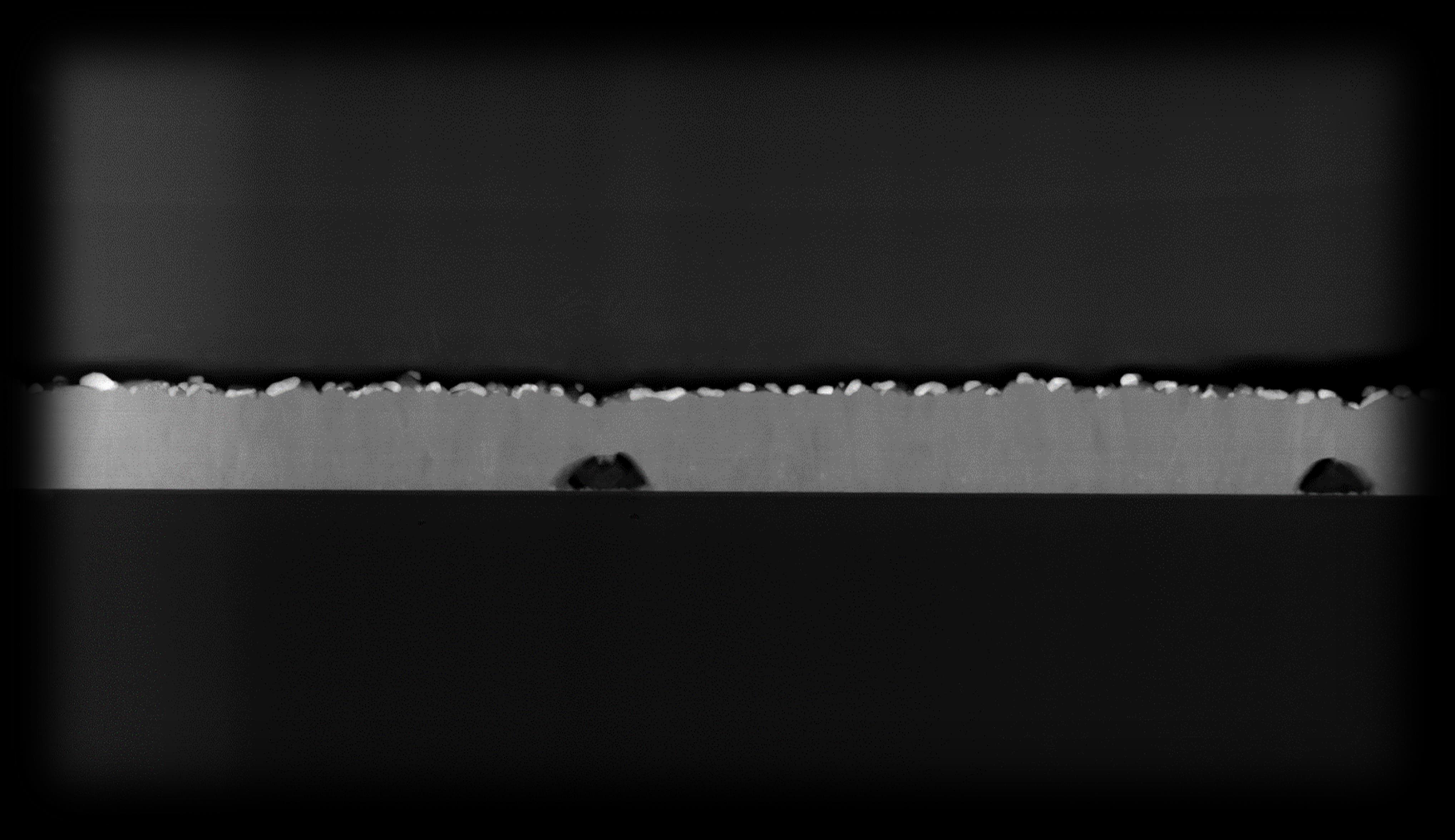
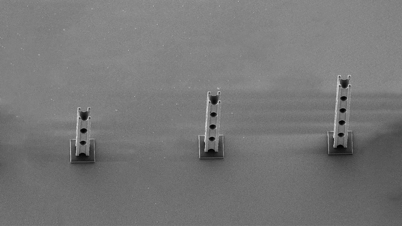
High density arrays of silicon wedges bound by {111}-planes on (100) silicon wafers have been created, by combining convex corner lithography on a silicon dioxide hard mask with anisotropic, crystallographic etching in a repetitive, selfaligned multiplication procedure. A mean pitch of around 30 nm has been achieved, based on an initial pitch of approximately 120 nm obtained through displacement Talbot lithography. The produced high density arrays of wedges offer a promising template for the fabrication of large arrays of nano-devices in various domains with relevant details in the sub-10 nm range
(ACS Applied Nano Materials 2022, 5, 10, 15847-15854, DOI: 10.1021/acsanm.2c04079)
In two joint PhD degree projects, methods to obtain wafer-scale microparticle assemblies were studied. Rubbing a particle suspension over a patterned surface with a grooved PDMS slab turns out to be one of the most successful techniques, whichwas shown to work for silica and polystyrene particles. The method may find applications in the production of medical devices, antireflective coatings, or microfluidic devices for chemical analysis or catalysis. The research was highlighted on the cover of the journal Langmuir.
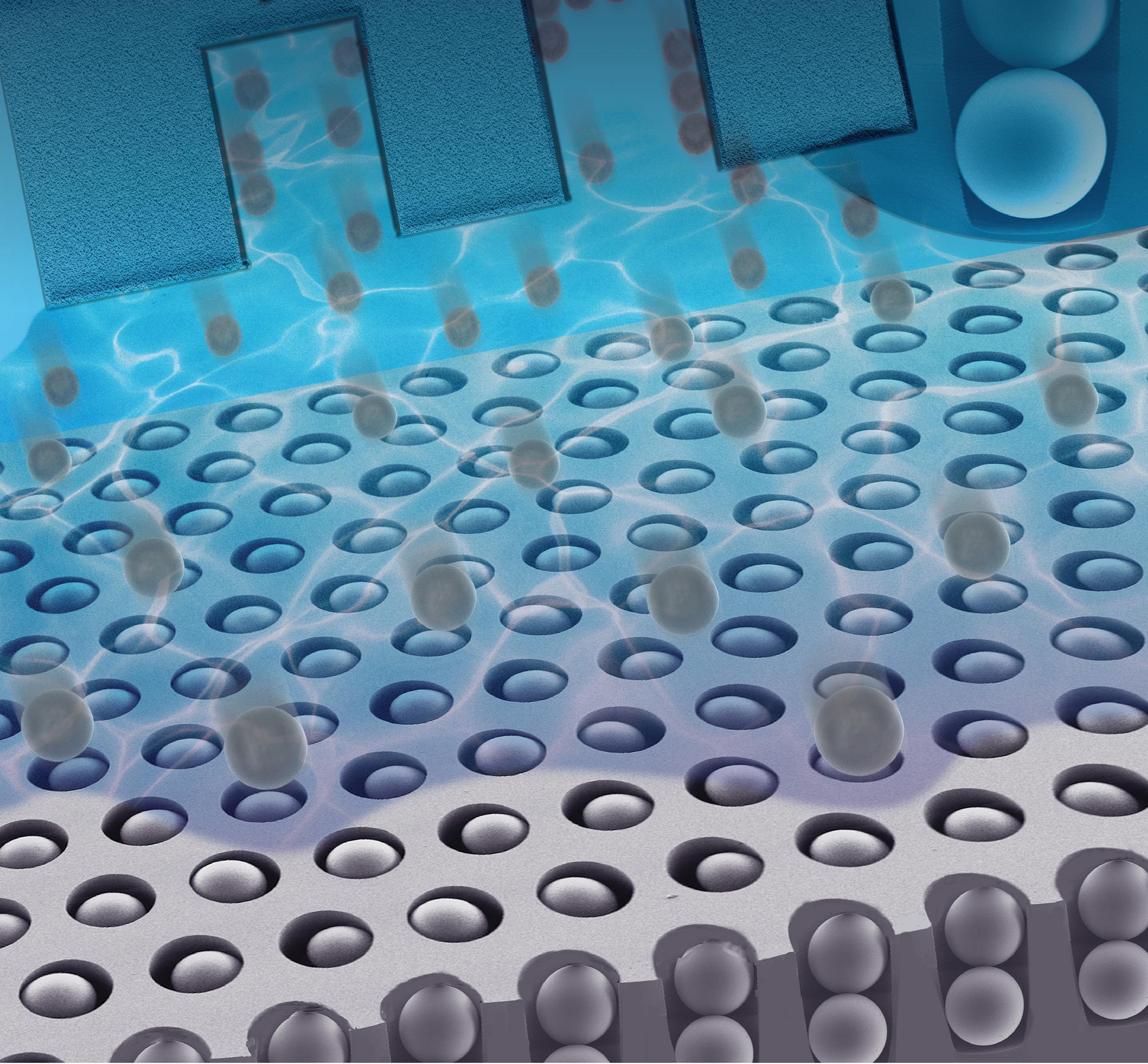
S. Verloy et al. Langmuir 2022, 38, 25, 7709-7719; https://doi.org/10.1021/acs.langmuir.2c00593
Han Gardeniers, Mesoscale Chemical Systems, in collaboration with Gert Desmet, VU Brussel
 Adaptive Quantum Optics, Jan Klärs
•
We demonstrated experimentally that low-buckled epitaxial germanene (the germanium analogue to graphene) is a quantum spin Hall insulator with a large topological gap and robust metallic edge states.
• The application of a transversal electric field induces a topological phase transition in germanene, allowing the topologically protected edge states to be switched ‘on’ and ‘off’ at will.
 Pantelis Bampoulis, Physics of Interfaces and Nanomaterials
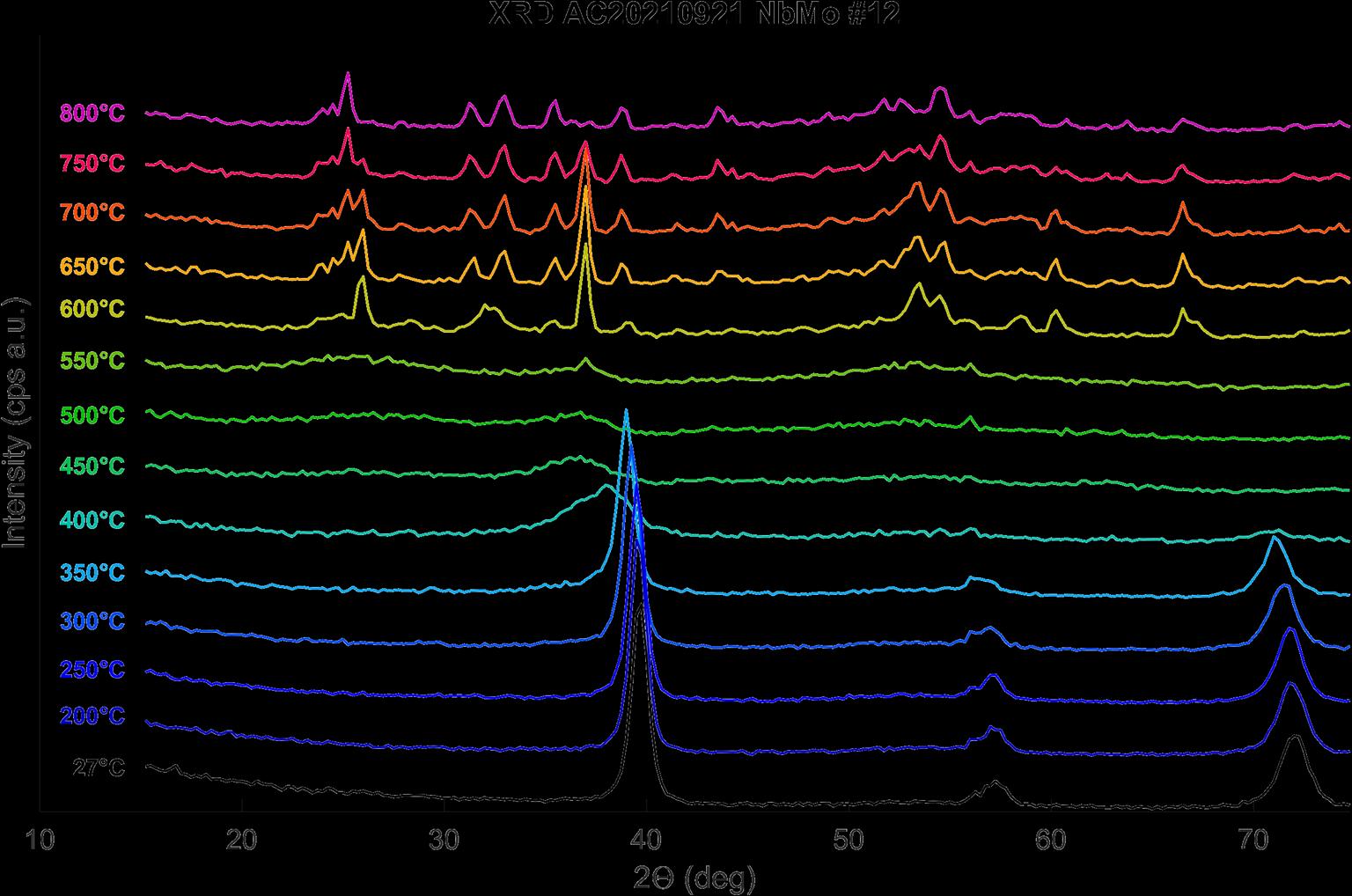
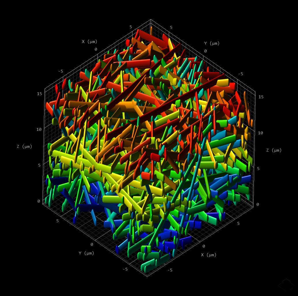
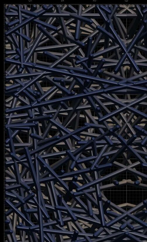
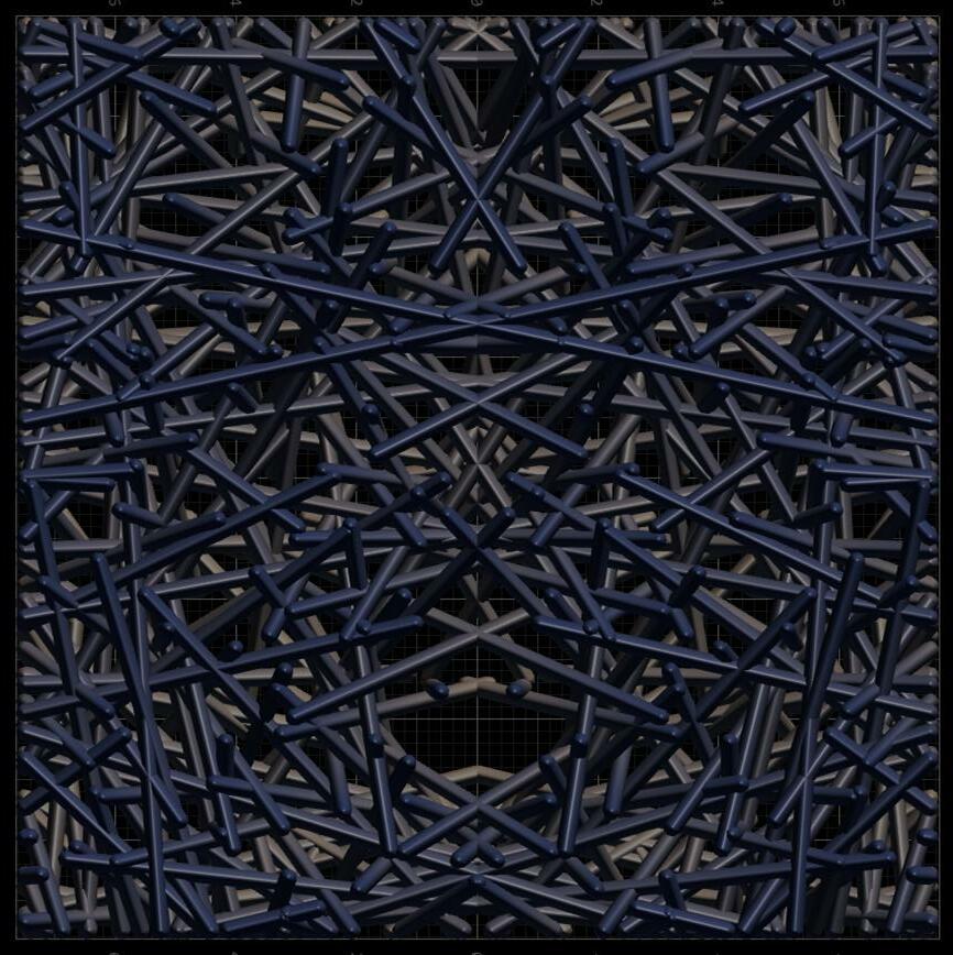
 MarcDhalle,HermantenKate,AnnaKario,ArendNijhuis
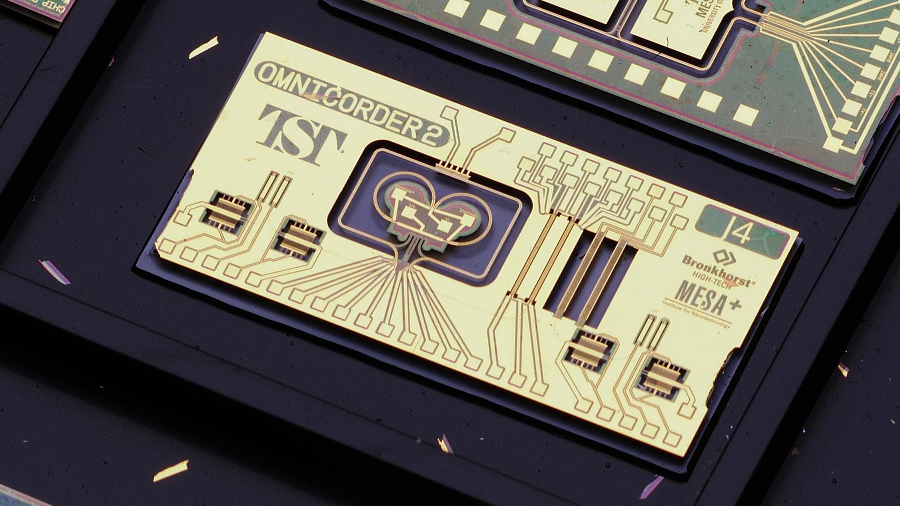 Joost Lötters − Integrated Devices and Systems
Many applications in for instance the medical, chemical and biological fields show a need for modular microfluidic handling systems. These systems enable accurate, real-time and in-line flow control and analysis of small quantities of (mixtures of) gases and liquids. We work on microfluidic handling systems which are integrally designed from the system perspective. Different functionalities, such as modules for flow measurement, -control, -dosage and -analysis, can therefore easily be integrated.
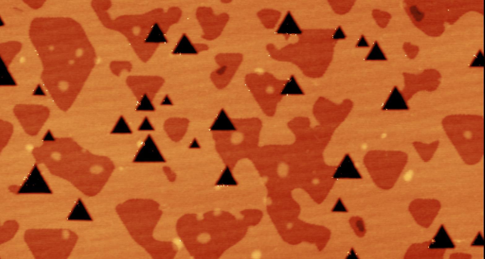
PtGe eutectic droplets move in a thermal gradient on Ge(110). Phys. Rev. Mat. 5, 105601 and 125602
 Arie van Houselt, Physics of Interfaces and Nanomaterials
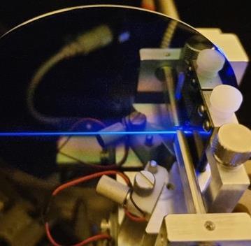
 Prof. K.-J. Boller, Laser Physics and Nonlinear Optics group


 Jelmer Renema & Adaptive Quantum
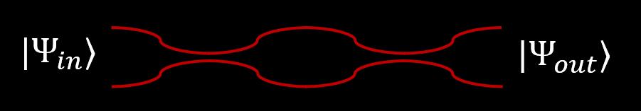
We have performed a simulation of quantum thermodynamics on a photonic processor, tackling one of the core questions of quantum physics: how do we reconcile unitary evolution of quantum states with the second law of thermodynamics.
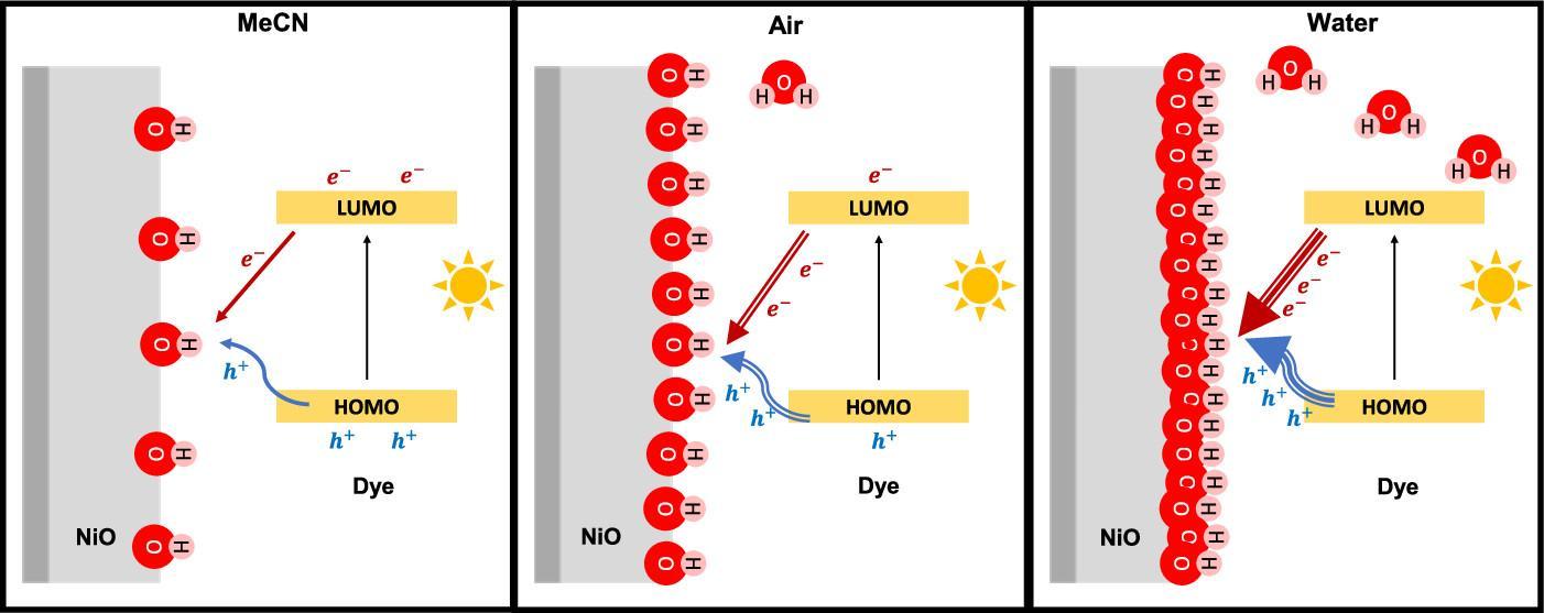
Zhu, Frehan, Mul, Huijser, PhotoCatalytic Synthesis group
J. Am. Chem. Soc. 2022, 144, 24, 11010–11018
Photoelectrochemical cells containing photocathodes based on functionalized NiO show a promising solar-to-hydrogen conversion efficiency. We studied the photoinduced charge transfer processes at the photocathode/electrolyte interface and demonstrate that surface hydroxyl
 Wouter K. den Otter, Multi Scale Mechanics
Simulations and experiments where used to study the permeability of microfluidic channels containing (dis)ordered arrays of floor-to-ceiling pillars, as used in chromatography, This work is a collaboration with Thejas Hulikal Chakrapani, Stefan Luding, Hanieh Bazyar and Rob Lammertink.
We designed and built a microreactor enabling X-ray imaging for a wide range of catalytic systems under real operating conditions, thus facilitating the fundamental understanding of heterogeneous catalysts and their design.
 BIOS lab on a Chip group - Luca Carnevale, Wouter Olthuis, Remco Wiegerink, Mathieu Odijk
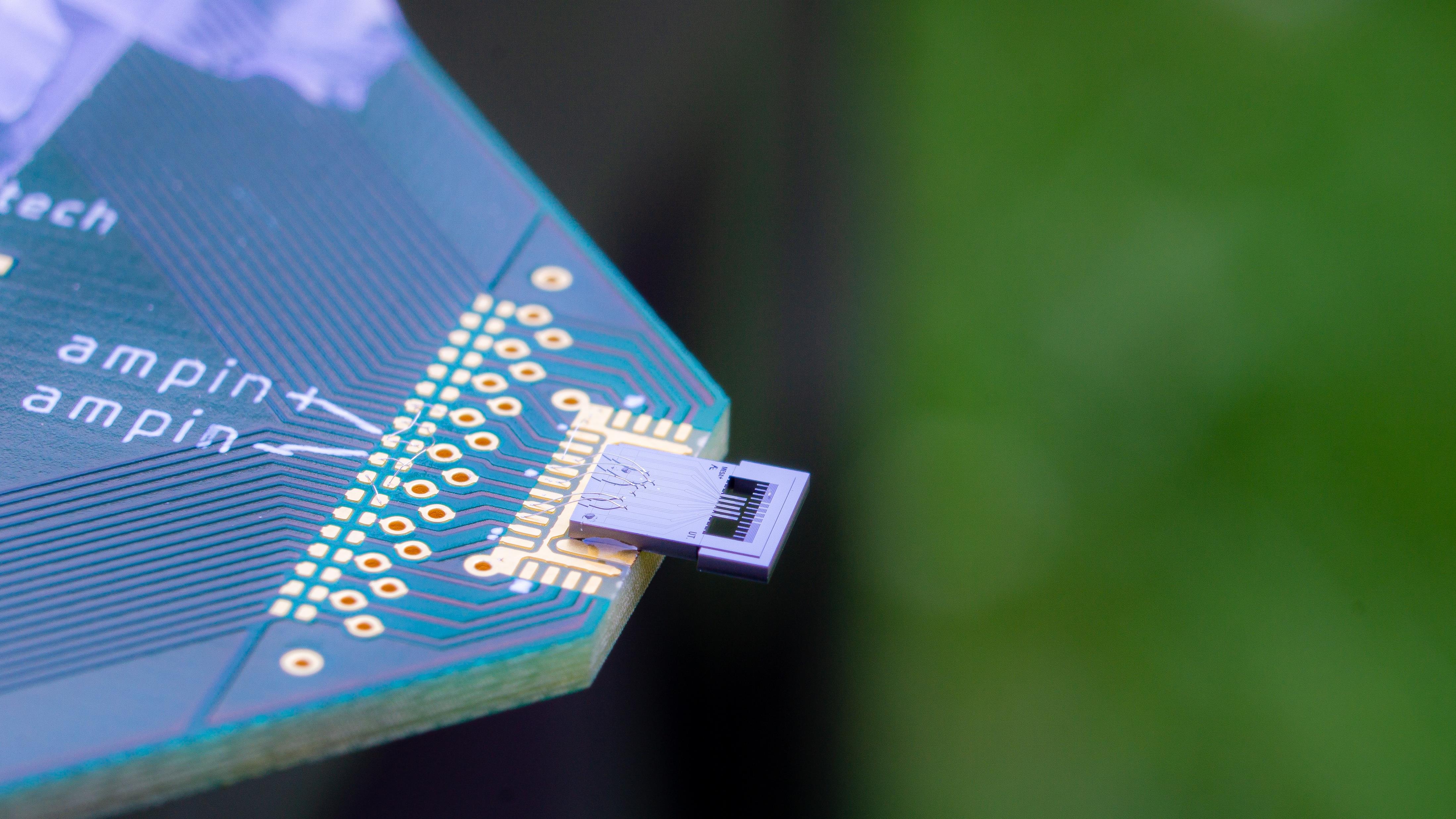
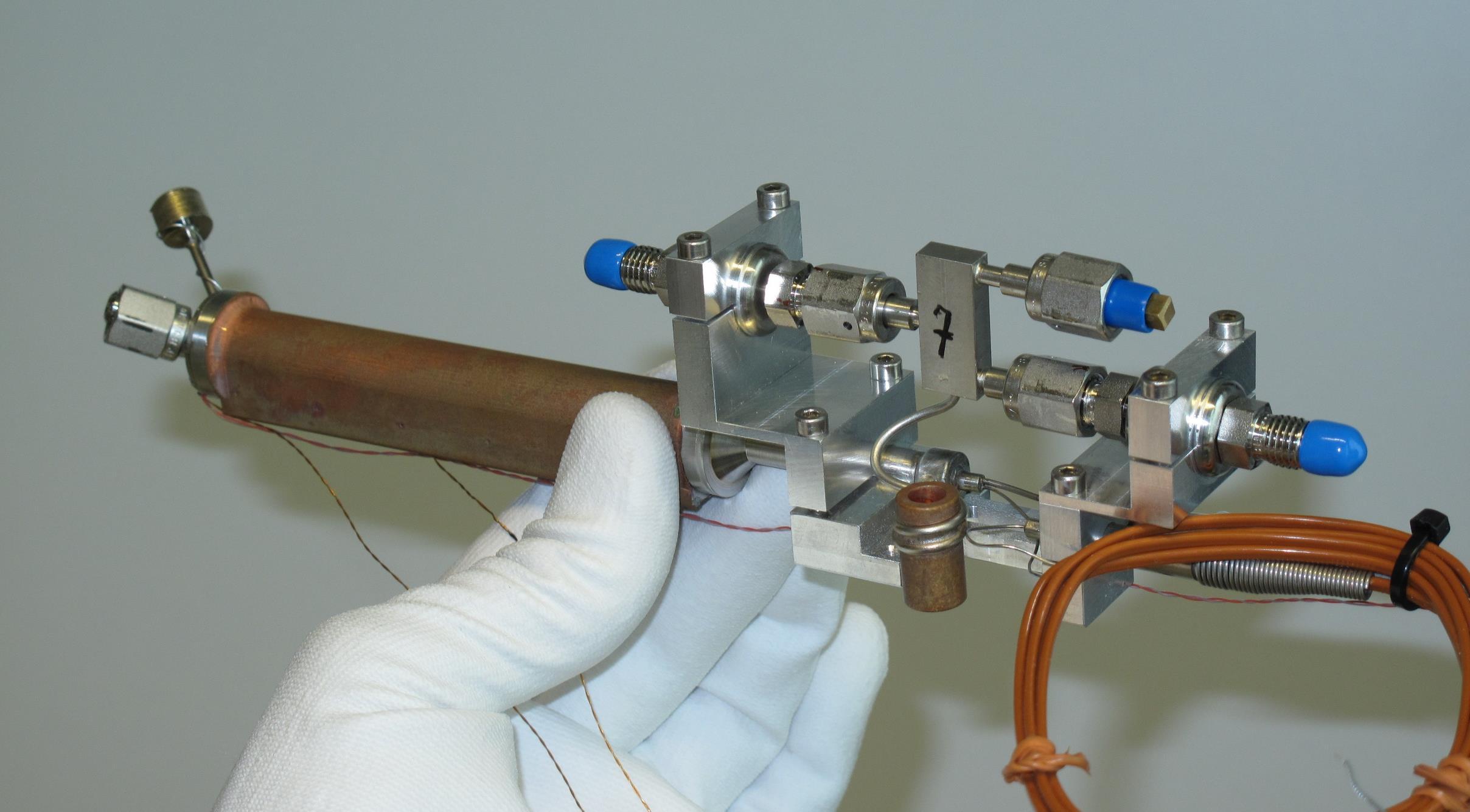 Marcel ter Brake: Vibration-free cooling for Big Science projects, Quantum Technology, Cryo-EM for life science, Space and ground-based optical instruments


• surface charge mapping in the dark and under constant illumination
• rational design of materials and optimized operation conditions
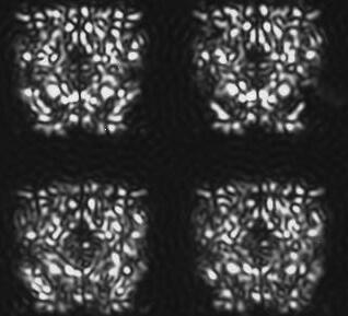
 Pepijn Pinkse & Adaptive Quantum Optics
Advances in nanofabrication techniques (Direct Laser Writing) allow us to manufacture deterministic scattering media, such as the mirror-symmetric one as shown over here. With this deterministic control over previously assumed inherently random media, we find applications in anticounterfeiting.


Efficient lubrication is essential for smooth and sustainable operation of machinery. Lubrication greases release tiny bits of oil to enable reliable bearing operation for years. New operating regimes e.g. in electric cars and wind turbines require durable high-performance lubrication. PCF, SPC, and TPM together with SKF, Shell and other partners use functional polymer brushes to explore novel concepts for controlled-release functional lubricants
– a fascinating challenge for the design of soft functional materials
 Physics of Complex Fluids (Frieder Mugele) & Sustainable Polymer Chemistry (Sissi de Beer) in collaboration with Tribology Based Maintenance (Piet Lugt)

I.A. Makhotkin, XUV Optics
• Nanoscribe was used to print compound refractive lenses (CRL)
• Test are done on the CRLs for focusing of soft Xray beams at synchrotron X-ray microscopy beamlines.
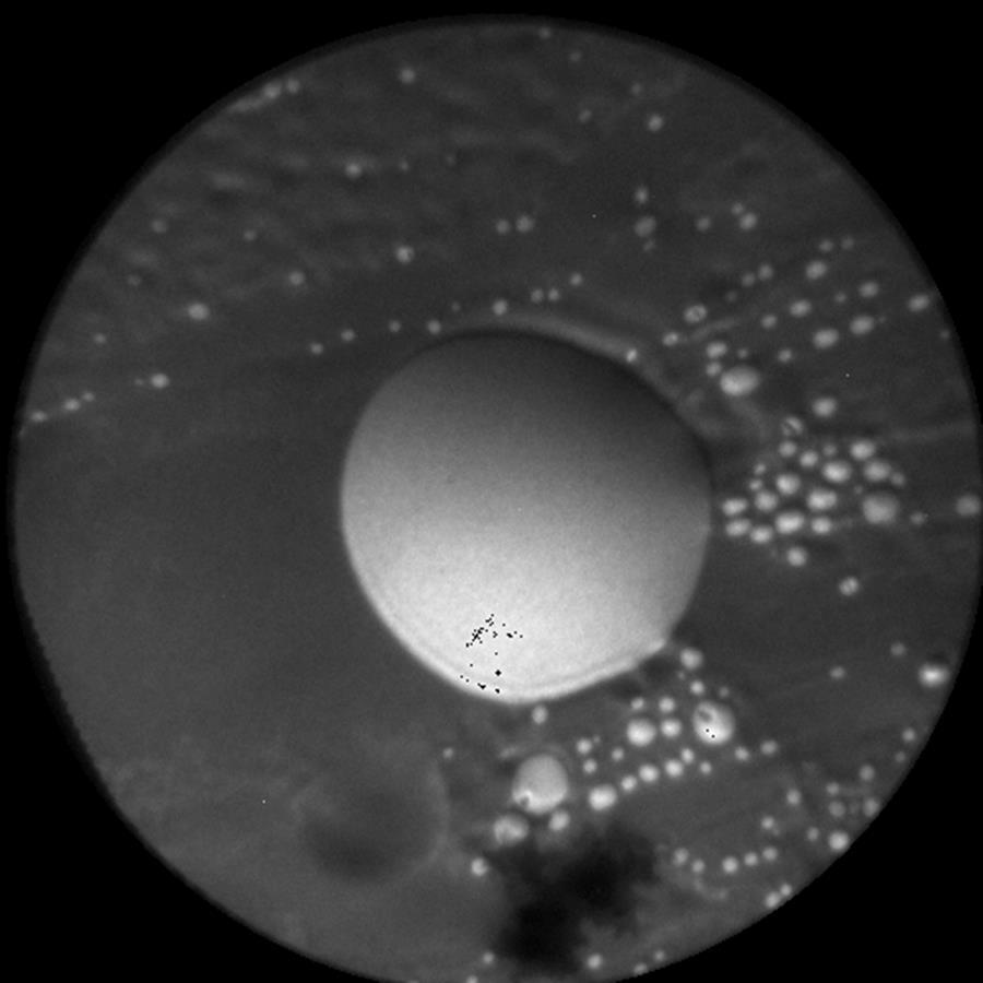
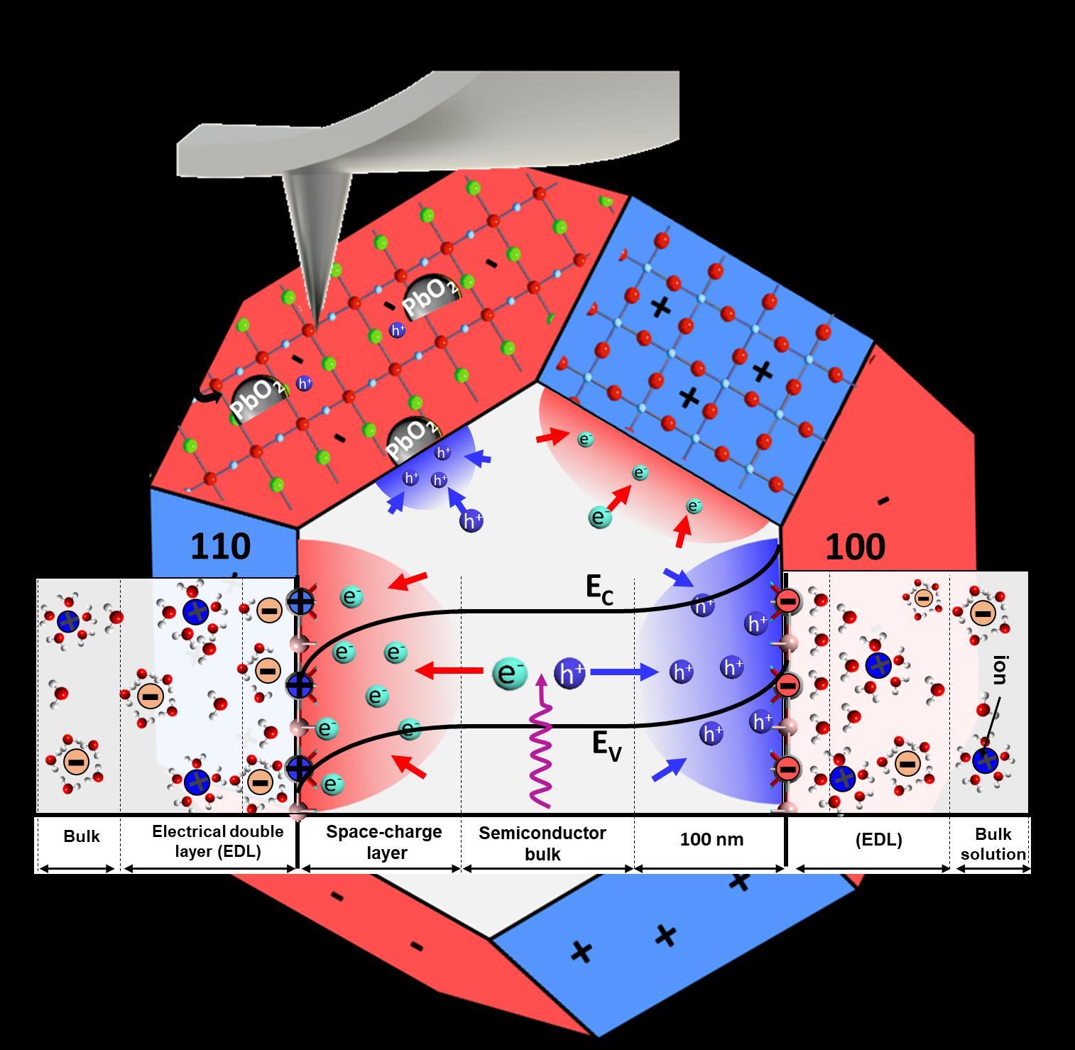
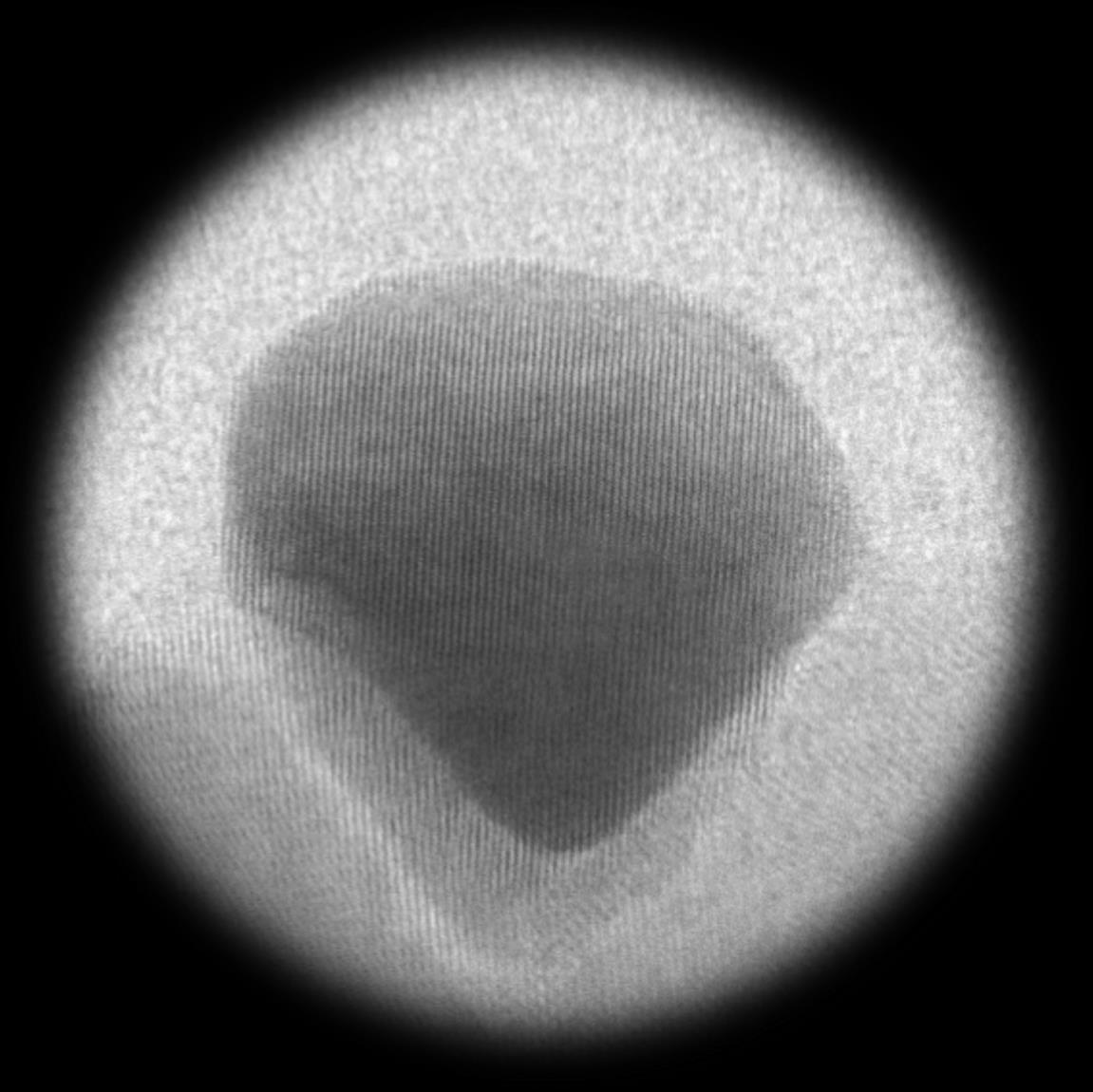
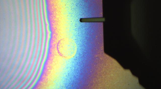
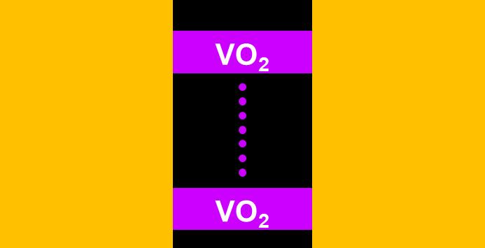
A reversible semiconductor-to-metal transition of VO2 is observed while applying a controlled amount of mechanical pressure by a nanosized metallic probe using an atomic force microscope.
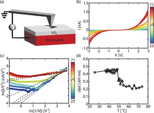
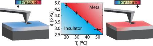
Representation of the experimental setup and Measured phase diagram.
The median I(V) curves recorded at different temperatures (b) and plotted on a ln(I/V2) versus ln(|1/V|) scale (c). Obtained barrier height parameters (d).
MercuryDPM is the software for fast and flexible simulations of particulate systems. It is developed by groups MSM and PMG (T. Weinhart, I. Ostanin and A. Thornton at TFE-ET).
In 2022, the code was enriched with a number of new features:
• A set of advanced contact models for multiphysics problems
• Modeling multiphase problems (e.g. spray wetting)
• Mercury Cloud – scalable on-demand computations via web interface

• Advanced statistical modeling of granular assemblies
• Nonspherical particles
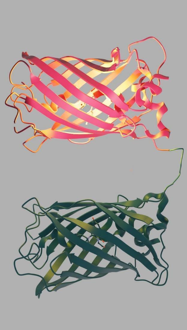
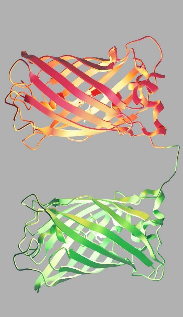
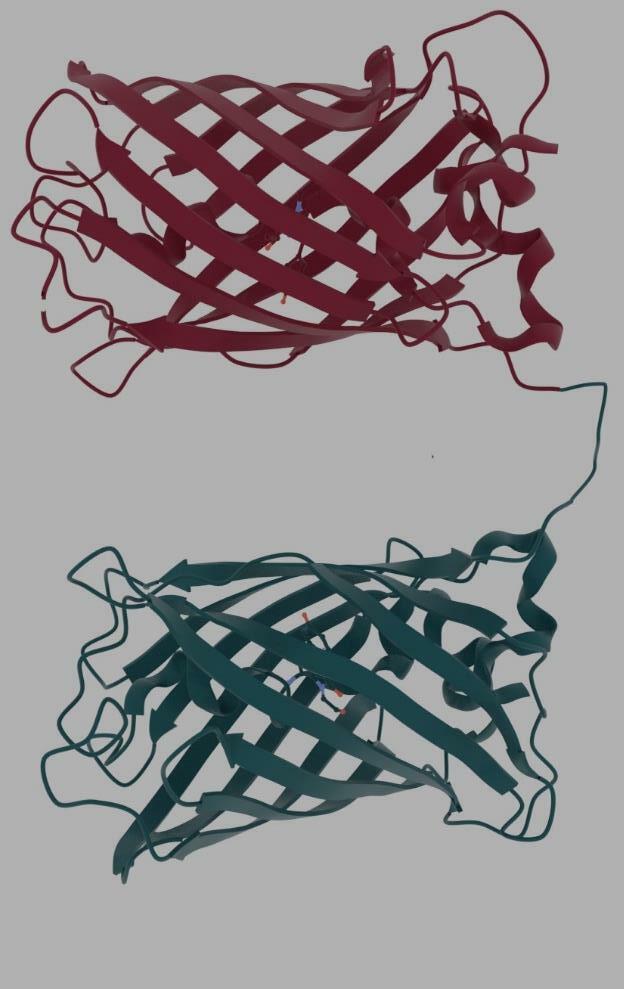 Mireille Claessens & Christian Blum - Nanobiophysics
• Quantification of dark fractions in fluorescent proteins • Enabling quantitative microscopy
Heesink et al. J. Phys. Chem. B. 2022


A set of free-standing zone-plates matched to a grating (for long wavelengths at the top and for shorter wavelengths at the bottom) for simultaneous spectral andspatialunravellingofEUVlightsources
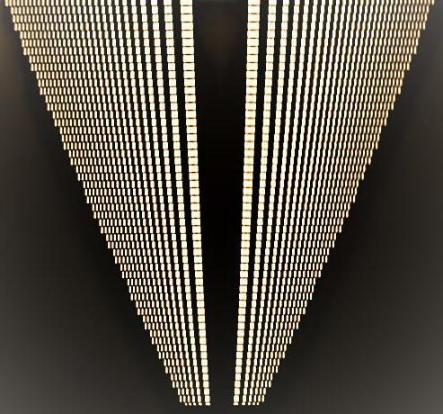 Muharrem Bayraktar - XUV Optics Group