
Annual Report 2022
We work with a network of over 40 companies, representing strategic UK sectors including telecommunications, healthcare, defence and aerospace, to support the rapid commercialisation of innovative photonics manufacturing technologies.
Together, we are combining our expertise and state-of-the-art experimental facilities to:
■ Lead research in core photonics platform technologies: silica optical fibres, III-V semiconductors, silicon photonics, 2D materials and metamaterials.
■ Develop integrated manufacturing processes, making it simple and efficient to incorporate photonics into high-value systems.
■ Fund early stage research into cutting-edge manufacturing technologies.
The Future Photonics Hub is a partnership between two leading UK research institutes, the Optoelectronics Research Centre at the University of Southampton and the EPSRC National Epitaxy Facility at the University of Sheffield.
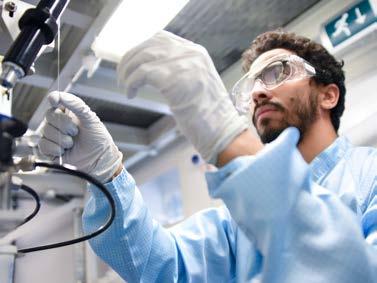
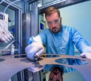
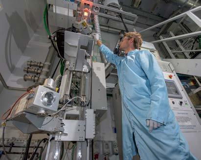
| Introducing the Future Photonics Hub Contents Introducing the Future Photonics Hub 03 Our mission 04 Executive summary 06 Microsoft acquisition of Lumenisity 08 Shaping the Future of Photonics at the Hub Industry Day 10 Rising to the challenge of the global shortage of semiconductors 12 The ultimate enabling technology 16 Core technology platforms 18 Innovation Fund 20 Research income 24 National leadership 26 Bringing photonics research to more diverse audiences 28 Technical reports 32 The team 54 3 4
We aim to secure the UK’s position as a leading innovator in the high value global photonics market by transferring new, practical and commercially viable process technologies to industry.
We respond to the needs of industry by creating new photonics materials, devices and components, designed to be easy to manufacture and integrate with existing technologies.
We bridge the gap between academic research and industry requirements, uniting the UK science base with industry and funding agencies to co-invest in manufacturing.
We use innovation in light technologies to accelerate growth in the UK’s £14.5 billion photonics industry* and support UK manufacturing output across key global market sectors.
| Our mission
5 4
*Source: The Photonics Leadership Group (PLG), July 2021.
Received many prestigious international awards, including Sir David Payne’s VinFuture Foundation Grand Prize and Professor Nikolay Zheludev’s Michael Faraday Gold Medal and Prize.
In the seven years since inception we have more than quadrupled the scale of our initial Government investment. We have generated more than £20 million of income from industry and are working on 87 research projects to help bring new photonics technologies closer to market. We have also been awarded an additional £23 million in competitively won grant funding to further accelerate next generation manufacturing related research.
Worked with companies, such as IQE, to improve the facial recognition systems that are used in smartphones.
Held our first in-person Hub Industry Day since the COVID-19 pandemic.
Sold spinout company Lumenisity Limited to Microsoft.
Provided photonics training and kits to teachers that could potentially benefit 7,500 students in the next three years.
Made breakthroughs in hollow-core fibre technology by exploring the impact of gas flow on optical and mechanical performance.
Achieved breakthroughs in semiconductor technology by extending research into mid-infrared wavelengths.
Visited Westminster with the aim of improving government engagement with photonics.
Achieved major industrial contracts worth £3M, including one with Honeywell (USA) worth £1.1M.
“It has been an exceptionally busy year for the Hub with many exciting changes resulting from commercial success. The Hub has attracted considerable leveraged funding, more than quadrupling the initial £10M granted by EPSRC. Our start-up Lumenisity has been acquired by Microsoft, who become a valued member of our local “photonics valley” of companies. We look forward to working with them in the future to bring hollow-core fibre to the telecoms volume market.
It has also been an excellent year for global recognition of Hub staff. Professor Nikolay Zheludev received the Michael Faraday Gold Medal and Prize and I was awarded the VinFuture Foundation Grand Prize. The status of Fellow was conferred by Optica on three of our staff and three were listed in the Photonics 100 of global innovators, cementing our position as one of the leading Institutes in the world of photonics.
We have extended the duration of the Hub for a further year to take account of time lost during the COVID-19 pandemic and this gives us time to bid for a new hub in photonics. Photonics is a £14.7 billion industry in the UK with a strong manufacturing base, so there is an obvious need for a research Hub in the sector.”
Professor Sir David Payne Principal Investigator, The Future Photonics Hub
| Executive summary
Together we are maximising the impact of Government investment and continue to make great strides in uniting the UK photonics community.
In 2022 we have
7 6
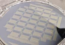
Lumenisity was spun out from the University of Southampton in 2017. It has gone from strength-tostrength as a leader in hollow-core fibre (HCF) technology leading to its acquisition by Microsoft in 2022. The acquisition will enable Microsoft to install HCFs to further optimise its cloud infrastructure and to serve their customers with strict latency and security requirements. In return, Microsoft’s support will enable researchers to fulfil this technology’s full potential by continuing to unlock new capabilities in communication networks.
Lumenisity’s core founders –Professors David Richardson, Francesco Poletti and Marco Petrovich – spent over a decade developing HCF at the Optoelectronics Research Centre (ORC) at the University of Southampton and began looking to commercialise their research. With the help of a seasoned Chairman and CEO, Dr David Parker, the company was established in 2017. Academics based at the university worked with Lumenisity to commercially develop HCF technology through the Future Photonics Hub. The challenge was to improve the fibre manufacturing process. By the time of Microsoft’s acquisition in December 2022, the company had grown significantly, successfully commercialised their product and built a dedicated facility in the Southampton area.
Lumenisity has become the global leader in HCF for telecommunications. HCFs allow data to travel 50 per cent faster than in traditional solid core fibre. With increasing global volumes of data and requirements for faster speeds, the increased bandwidth and enhanced network quality of HCF provides a basis for next generation communications.
Lumenisity is the only optical cable supplier currently capable of producing and cabling HCFs of low enough loss for telecommunications over long distances. Last year euNetworks, a European bandwidth infrastructure company, installed a new 45km ultra low latency route to Basildon including Lumenisity CoreSmart® HCF cable; this route is now 30 per cent faster than all equivalent fibre routes. As a result, the UK is well ahead of the USA, Japan and China in the telecommunications sector, with the University of Southampton driving many major advances in this field.
2022 has been a landmark year for Lumenisity with the company being recognised in a number of international awards. Professor David Richardson, Deputy Director of the ORC and Co-Investigator of the Hub, was recognised for his role in founding Lumenisity in The Photonics100, a newly-
launched international initiative by Electro Optics that celebrates the industry’s most innovative people. He said: “I am delighted to have been recognised in this way by my peers for my enterprise and research contributions. The fact that three members of the ORC have been included in this top 100 list highlights the important role Southampton plays within the international photonics community.” Furthermore, Lumenisity has won the Best Fibre Component Product for their NANF® CoreSmart® HCF cable in the European Conference on Optical Communication (ECOC) Exhibition Industry Awards for two consecutive years, indicating the strength and singularity of HCF technology.
The development of Lumenisity’s new fibre fabrication facility in Romsey (UK) was also completed this year. It is the world’s first dedicated HCF manufacturing facility and it will enable the company to scale up the manufacture of HCF. This will benefit a broad range of industries including healthcare, financial services, manufacturing, retail and government and secure Lumenisity’s place as the leading name in HCF technology.
| Microsoft acquisition of Lumenisity 9 8
The Future Photonics Hub has played a significant role in growing the photonics sector in the UK and Lumenisity is one of its greatest success stories.
Future
all existing limits. The potential of photonics has hugely exciting application opportunities for external collaboration, particularly in telecommunications, sensing, quantum, healthcare and biomedical imaging.
David said: “The event was a unique opportunity to promote the excellent science base and outcomes emerging from the ongoing Hub programme to key external stakeholders. This will help to develop a pathway to manufacturing for next generation photonics technologies and realise the importance of photonics becoming an enabling technology in every field.”
spend time understanding the challenges they face and where next-generation photonics can have impact on their organisation.
Professor Mark Spearing, VicePresident of Research and Enterprise at the University of Southampton, emphasised this in his closing remarks, recognising that the Hub is a crucially important initiative that attracts inward investment in innovation.
In September, key representatives from academia, industry, government, and research and technology organisations gathered to hear from the Hub’s expert scientists about the important advances they have been making in photonics manufacturing research. These have been in areas such as optical fibres and lasers, mid-infrared photonics, silicon photonics and advanced materials.
The delegates were also part of a forum discussing the challenges and opportunities for UK photonics manufacturing and listened to a keynote presentation from Dr John Lincoln, CEO of the Photonics Leadership Group, focusing on Photonics for Net Zero – growth and opportunities in the post-COVID-19 era. With an increasing reliance on data, the photonics industry faces a huge challenge in meeting this demand in a sustainable way. John emphasised the importance of being
proactive, rather than reactive, in the face of this challenge.
Hub Deputy Director and Manager Professor Gilberto Brambilla said: “The EPSRC-funded Future Photonics Hub Industry Day was an opportunity to help shape future research to the benefit of the UK economy in response to the government’s Innovation Strategy where electronics, photonics and quantum is highlighted as one of the seven technology families that are helping the UK maintain its status as a leading innovator in a highly competitive, high-value global market.”
“We know the astonishing range of innovative ideas that emerge when industry and universities come together to think about manufacturing, and we recognise that scientific discovery is only part of the solution to a successful product.”
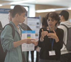
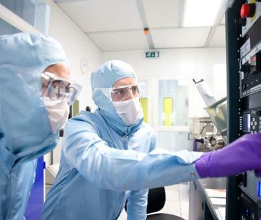
The Industry Day also featured a showcase of exhibits from photonicsrelated researchers and companies. Technology posters provided visitors with the opportunity to find out more about the technology platforms they were interested in. Delegates also got the chance to network and explore collaborative working and tour the Zepler Institute’s world-leading cleanroom facilities. Over 20 visitors took part in the cleanrooms tours and many others enjoyed a virtual tour using a headset in the exhibition hall.
Hub Co-Investigators and Deputy Directors of the Optoelectronics Research Centre (ORC) Professor Graham Reed and Professor David Richardson led a talk sharing their plans for the future. The Hub has the potential to take photonics research even further by incorporating artificial intelligence, focusing on device integration for a range of applications, and working towards ultrawideband photonics exceeding
Graham added: “It was fantastic to see so many of our friends and collaborators at the Future Photonics Hub event. I look forward to working with them on some of the interesting future projects that we discussed.”
Innovate UK’s Iain Mauchline, Innovation Lead – Electronics, Sensors and Photonics shared a range of exciting funding mechanisms for photonics as a key enabling technology for delivering strategic themes such as Net Zero and health and wellbeing. He also talked about the crucial importance of academia and industry working together to take new ideas from the lab into production at scale.
The Hub helps industry access the latest photonics innovation by engaging with a large network of external companies. It provides access to leading researchers who
| Shaping the Future of
at
The
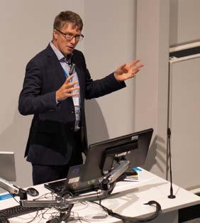
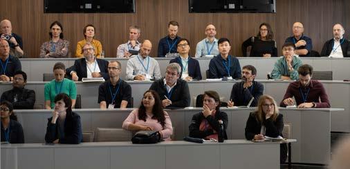
Photonics Hub’s first Industry Day since the pandemic was a resounding success with nearly 150 delegates coming together to discover and influence the future of the photonics innovation landscape.
Photonics
the Hub Industry Day
Key representatives from academia, industry and the government attended the Hub Industry Day
Dr John Lincoln delivering his talk regarding Photonics for Net Zero
10 11
Staff and students discussed the research that was exhibited
They are used in communications infrastructure, artificial intelligence, robotics, healthcare, military technology, quantum and cloud computing, and everyday consumer devices such as white goods and smart meters.
But during the COVID-19 pandemic, supplies were seriously disrupted and the world is now facing a semiconductor shortage.
As the UK government is preparing to help boost the British semiconductor industry by publishing a UK Semiconductor Strategy, we take a look at key semiconductor research and development that is being carried out by the Future Photonics Hub, some of which is being made available in an open source way by CORNERSTONE, a UK research foundry service providing Silicon Photonics circuits and devices, operated by the University of Southampton.
Developing Silicon Photonics
Currently the biggest market for semiconductors is silicon electronics, however, there is increasing demand in certain application areas for Silicon Photonics that enables the high volume, low-cost and highperformance production of photonic devices and circuits which utilise and manipulate the properties of light rather than electrons.
Silicon Photonics at nearinfrared wavelengths has already revolutionised data communications, and numerous other applications are emerging. However, some of the emerging applications require longer wavelengths and different waveguiding platforms.
Semiconductor technology for these longer wavelengths is being developed within the Hub and could have significant global impact in areas such as environmental sensing, early diagnosis of cancer and therapeutic drug monitoring.
Hub academics are exploring semiconductor technology to extend research into mid-infrared wavelengths – known as the fingerprint region – that could be used to create sensors at the chip scale.
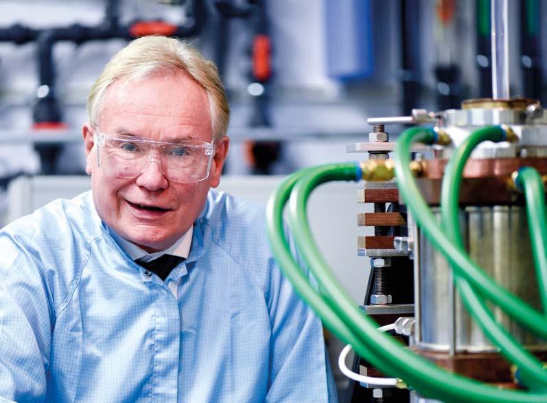
Professor Graham Reed, a Hub Co-Investigator and Director of CORNERSTONE, has recently been part of a Government delegation to the USA to share the UK’s semiconductor capabilities. He said: “We are carrying out research into the use of semiconductors in silicon photonics to develop spectrometers on a chip that could spot unique identifiers in biological and chemical molecules. These new spectrometers would be smaller, cheaper, more manoeuvrable, more useable, and potentially more sensitive than the current large, bench top tests that may only be available in centralised
|
Rising to the challenge of the global shortage of semiconductors
Semiconductors are essential ingredients of almost every electronic and photonic device on the planet.
13 12
Professor Graham Reed, a Hub Co-Investigator and Director of CORNERSTONE
| Rising to the challenge of the global shortage of semiconductors
testing laboratories, adding delays to testing outcomes. Miniaturised chip scale tests could be deployed locally, at the point of care, to dramatically speed up results.”
“Our Hub colleagues in Sheffield are also exploring the integration of lasers onto these new platforms where appropriate, so that the chips will have the full on-chip sensing capabilities.”
The synergy between the Hub and CORNERSTONE means that this technology can then potentially be made available to CORNERSTONE users in both academia and industry.
CORNERSTONE Coordinator
Dr Callum Littlejohns said: “As we have done with previous research from the Hub and elsewhere, we take these latest technologies and offer them licence free and open source for the benefit of our clients. This flexibility enables them to try out new devices and novel ideas, or to develop new prototypes.”
Global impact
The Hub’s semiconductor Silicon Photonics research and development is already feeding into a multimillionpound research programme - MidInfrared Silicon Photonic Sensors for Healthcare and Environmental Monitoring (MISSION) - that is
spearheading the creation of new sensors that monitor drugs, speed up cancer detection and measure the impact of climate change.
Led by Southampton’s Zepler Institute (with partners York, Sheffield, University Hospital Southampton NHS Foundation Trust and the National Oceanography Centre Southampton), MISSION aims to use spectrometers on a chip to solve societal challenges and transform people’s lives in three key areas:
■ Environmental monitoring of gases
■ Therapeutic drug monitoring by healthcare professionals
■ Early stage cancer detection
Environmental monitoring of gases – focusing explicitly on oceans and how sensors on a chip can be used to identify problematic gases in the oceans. Currently these gases are typically monitored by deploying ships with numerous large sensors, but sensors on a chip could be put on robots, drones or even dropped directly into the sea. This could enable more, and previously inaccessible places, to be monitored.
Therapeutic drug monitoring for healthcare professionals – currently blood samples have to be sent away to a laboratory to measure drug concentrations. Sensors on
a chip could enable point-of-care diagnostics allowing doctors to administer more accurate doses of drugs and optimise the effectiveness of drugs in real time.
Early stage cancer detection –current test equipment is typically very large and/or expensive, meaning patients have to be tested in hospital and the number of people that can be evaluated each day is limited. This also requires a wait for results. Using a spectrometer on a chip would enable more people to be diagnosed more quickly and therefore earlier. The lower-cost, smaller equipment could potentially be available in every doctor’s surgery, every hospital ward and perhaps even in people’s homes.
The future
The processes being developed at Southampton have the potential to be used in a range of different applications. Spectrometers can be used to measure numerous species from gases to explosives, so in principle it is very widely applicable.
Through CORNERSTONE, it is not only academics at Southampton who can benefit from the technologies that are developed; they are available to anybody via the open source platform.
15 14
Photonics is the science and technology of light. Although most people do not realise it, photonics technologies are widely integrated into products and systems across a broad range of sectors.
Here are just a few examples of the many applications of photonics technologies.
Enabling key industry sectors
Harsh environment sensors for oil & gas
Value £14.5bn industry value to the UK economy
Employment
76,700 people employed across the sector
Laser-written diagnostics for healthcare
Optical fibres for high bandwidth telecommunications
LIDAR for autonomous vehicles and other imaging applications
Sensors for security
Silicon photonics for data centre communications
High power fibre lasers for green manufacturing
Detectors for space and remote sensing
Integrated photonics for quantum technology
Output £6.5bn total GVA £85,000 GVA per employee (vs UK manufacturing average of £67,000)
Growth 12% like for like growth over two years (5.8% CAGR)
UK photonics manufacturing industry
Putting the UK at the forefront of future industries
The UK is an international leader in photonics research. Our science base has already given rise to a globally significant market which continues to expand at an impressive rate.
Photonics technologies are both ubiquitous and transformative. The UK photonics manufacturing industry is growing, as are many other high-tech industry sectors enabled by photonics. Investing in future photonics innovation is critical to retaining the UK’s competitive edge in the £400 billion global photonics market and offers vast potential to stimulate wider economic growth.
Head-up displays for aviation
| The ultimate enabling technology
Photonics has near limitless uses and can be found in almost all of the products and services we use in everyday life.
Source: The Photonics Leadership Group (PLG), July 2021
17 16
We aim to develop the important ‘Pervasive Technologies’ identified in the UK Foresight report on the future of manufacturing, through carrying out research into four, carefully selected Technology Platforms: High Performance Silica Optical Fibres, Light Generation and Delivery, Silicon Photonics and the Large-Scale Manufacturing of Metamaterials and 2D Materials.
We also know that the key to producing low-cost components and systems is integration. Optical fibres, planar waveguides, metamaterials and III-V semiconductors cannot yet be combined in a cost effective, integrated manufacturing process.
Core Technology Platforms
1. Large-Scale Manufacturing of Metamaterials and 2D Materials
Developing cost-effective, reliable, and volume-scalable methods to fabricate these novel materials in order to enable their practical exploitation in applications such as telecommunications, displays and sensors.
Grand Challenge: Integration
Our consultations with over 40 companies, Catapults and Innovative Manufacturing Centres identified a clear business need to reduce the complexity of incorporating next generation photonics technologies in high value systems.
Integration is an industry wide issue which we have chosen to tackle as our ‘Grand Challenge.’
Our research capabilities
The Hub is a unique partnership between the Optoelectronics Research Centre (ORC) at the University of Southampton and the EPSRC National Epitaxy Facility at the University of Sheffield. It is this collaboration between two leading research institutes that ensures our work is characterised by scientific excellence and innovation. Together, we have an extensive and impressive track record in research and enterprise.
■ Our innovations navigate airliners, cut steel, mark iPads, manufacturing life-saving medical devices and power the internet.
■ Our optical fibres, invented and made in Southampton, are on the Moon, Mars and the International Space Station.
■ Our Silicon Photonics technology drives data centre communications.
■ Our epitaxial wafers and devices, produced in Sheffield, have enabled world-class semiconductor research in the UK since 1979.
■ Our combined portfolio of startups now exceeds 12 companies.
■ Our expertise is underpinned by our £200 million state-of-the-art fabrication facilities.
The drive to achieve integration is a ubiquitous theme uniting the world’s photonics industries. The photonics industry today can be likened to the early days of electronics when individual components were wired together, resulting in inevitable cost and scaling implications. Today’s photonics components are not yet compatible with a single manufacturing platform and this represents a major industrial challenge.
3. High Performance Silica Optical Fibres
Optical fibres are essential components in many photonic devices and systems - from sensing to amplifying light. The key challenge in manufacturing fibre is improving its loss, gain and power handling characteristics.
2. Light Generation and Delivery
User-driven manufacturing processes will increase the integration and unification of diverse manufacturing platforms in III-V epitaxy, metamaterials, Si-SOI fabrication methods and function fibre geometries.
4. Silicon Photonics
Achieving integration with optical fibres, light sources, and key processes in wafer level manufacturing to enable both novel devices and circuits such as low-cost transceivers for data centres as well as in emerging applications in midinfrared sensors, LiDAR and space photonics.
| Core technology platforms
We are developing new photonics technologies to fuel innovation. Our research is delivering solutions to manufacturing challenges and overcoming barriers to the widespread industry adoption of next-generation photonics.
19 18
Since 2016, we have awarded over £780,000 in grant funding to projects led by UK researchers offering new capabilities relevant to industry but outside of our core expertise.
Over the years we have awarded projects to researchers in institutions including the universities of Oxford, Cambridge, Bristol, Bangor, Southampton and Strathclyde.
In partnership
Our most recent call was launched in May 2021 in partnership with other EPSRC Future Manufacturing Research Hubs to jointly fund projects that exploit research synergies and allow access to a wider range of facilities and equipment.
Partnering with the EPSRC Future Manufacturing Research Hubs in Composites, Electrical Machines and Metrology, we offered up to £900,000 in funding to support a number of feasibility studies. £200,000 was awarded the following four photonics projects:
Novel, Embedded and Robust Optoelectronics to Value Engineer Precast Concrete Dr Brian Sheil, University of Oxford Practical sustainability goals can be achieved by minimising concrete consumption and extending the life of built infrastructure. This project explores the feasibility of developing and embedding novel ultra-low-cost optoelectronic sensing systems in precast construction elements for buried utility infrastructure. This project has developed novel optical ‘scattering’ interrogation techniques for monitoring Fibre Bragg grating (FBG) based systems. The developed system is low cost and was shown to be capable of achieving accurate measurement of multiple sensors. The team have also developed a novel methodology of embedded fibre optics in precast pipe sections to infer all salient forces using machine learning techniques and a virtual model of the pipe. Future research will build on this work to scale up to field-scale demonstrators and deployment of the technology on live construction sites.
The Future Photonics Hub
University of Southampton
University of Sheffield
Innovation Fund partners Heriot-Watt University
University of Bangor
University of Bristol
University of Cambridge
University of Oxford
University of Southampton with Imperial College, London
University of Southampton with Phoenix Photonics
University of Strathclyde
Industry partners
International industry partners by country
UK photonics industry activity
| Innovation fund
With support from our £1 million Photonics Innovation Fund, we are building a national network of academic partners, primed to respond to emerging industrial challenges with a wide range of expertise.
Sweden USA Canada China Japan South Korea Italy Germany Saudi Arabia 21 20
Disruptive Photonics Manufacturing for Ocean’s Dissolved Methane Monitoring


Dr Rand Ismaeel, University of Southampton
This project will further develop a novel writing technology to make the next generation of photonics marine sensors compatible with miniaturised autonomous underwater vehicles. They will create a cost-effective monitoring tool that can revolutionise how the oil and gas industry perform leak detection. The aim of this project is to explore a new concept of combined chemical sensing of methane, using optical fibre sensors. Spectroscopic detection of methane in water phase in a cryptophane host is an absolute novelty. Our data so far demonstrated up to 23-fold sensitivity enhancement from the pre-concentration. This will revolutionize current methods of ocean monitoring, enabling better mapping capabilities of oceanic methane emissions.
Pyroelectric PZT Thin Films Integrated on Si for Efficient IR Detectors
Dr Ioanna Bakaimi, University of Southampton Integrated detectors are needed to realise the full potential of silicon photonics in mid-IR sensing. This project aims to enable integration of efficient room temperature pyroelectric IR detectors on the silicon photonic platform using lowcost materials and a direct, reliable growth technique. This project has so far demonstrated that evaporative reactive physical vapor deposition can achieve such layers within suitable structures incorporating selected buffers without diffusion and reaction of highly reactive components.
Wafer-scale Manufacturing of Large Area Metasurfaces Using a Deep-UV Scanner
Professor Otto Muskens, University of Southampton
This project aims to enable deepUV wafer scanner and track tools to produce near- and mid-IR metasurfaces with applications in IR imaging and sensing. They aim to address the gap between smallarea demonstrators using e-beam lithography and Focused Ion Beam (FIB), and the need for large area, scalable manufacturing methods. A key advance achieved in the project is to manufacture metaoptics on a 200 mm semiconductor wafer production line, using Nikon Deep Ultraviolet (DUV) scanning lithography system and use this technique for the scale-up to high volume production. The volume manufacture capability has been demonstrated by forming 110 individual metalenses, each 12 mm in diameter, on a single 8-inch silicon substrate. The wafer-scale metalenses have been presented in several events in UK and have attracted strong interests from several industry partners for further research collaborations.
23 22
Innovating with industry for economic growth.
As national leaders in photonics manufacturing research, we stimulate collaborations between academia and industry throughout the supply chain.
We engage industrial influencers to raise awareness of the value of photonics, both in delivering transformational manufacturing technologies and driving economic growth.
We have secured significant income in all four Technology Platforms, working with companies across the photonics supply chain from component manufacturers to large end-users in a range of market sectors.
Our ramped-up activities under the Grand Challenge of Integration have also been supplemented by some targeted projects following the award of funding from the Defence and Security Accelerator (DASA).
Industrial income by Technology Platform
87 projects,
Technology Platforms 2016-2022
Total income January 2016 to December 2022
9 industry sectors 2016-2022: sensing, defence, photonics, data comms, storage, LIDAR for autonomous vehicles, aerospace, advanced materials and manufacturing
| Research income
£2m+
£20m+ Total
£23m
2022 industrial income
industrial income
36% competitively secured income
4
2016-2022
2016-2022 Total
£10m 23% core income
2016-2022 2016-2022
income
High-Performance
Light Generation and Delivery Silicon Photonics Large-Scale Manufacturing of Metamaterials & 2D Materials Integration £1,400,000 £20m 41% Industry income £1,100,000 £8,000,000 £3,800,000 £6,600,000 25 24
Silica Optical Fibres
Our role is to increase awareness and engagement with the ways photonics manufacturing research is tackling Grand Challenges, improving people’s lives and boosting productivity. We provide access to expertise which helps industry innovate and champion strategic investment that will drive social and economic impact.
International recognition
Many of those involved in the Future Photonics Hub received international awards in 2022 in recognition of their contributions to the field of photonics. Hub Principal Investigator, Professor Sir David Payne, whose pioneering work made the internet possible, was awarded the VinFuture Foundation Grand Prize in Vietnam. Sir David and his team developed the erbium doped fibre amplifier (EDFA) in the 1980s, one of the most significant developments in modern telecommunications.
Hub Co-Investigator Professor Nikolay Zheludev was awarded the 2022 Michael Faraday Gold Medal and Prize by the Institute of

Physics (IOP) in recognition of his discoveries and in-depth studies of new phenomena and functionalities in photonic nanostructures and nanostructured matter. He also received the prestigious Hagler Fellowship from the Hagler Institute for Advanced Study at Texas A&M.

Hub Co-Investigator Professor David Richardson and Hub Industrial Liason Manager Dr. John Lincoln were nominated for the Photonics100, a newly-launched international initiative by Electro Optics that celebrates the industry’s most innovative people. David was recognised for his role in launching Lumenisity, a spin-out company of the Airguide Photonics programme, while John was noted for his efforts in promoting the importance of a Net Zero economy in the field of photonics.
Engaging with government, academia and industry
In July, representatives of the Future Photonics Hub, along with 24 other separate organisations, visited Westminster with the aim of improving government engagement
with photonics. This event facilitated productive conversations with politicians, most notably MP Carol Monaghan, regarding the importance of photonics to the UK economy and the need for strong outreach programmes to encourage women into science, technology, engineering and mathematics (STEM).

Hub Principal Investigator
Professor Sir David Payne and Hub Co-Investigator Jayanta Sahu attended a prestigious UK delegation that visited India as part of the government’s UK/India Future Telecom Programme. They joined other distinguished representatives from academia and industry on the trip that aimed to establish potential collaborations to deliver transformational changes in future telecommunications networks. Sir David said: “The purpose of the trip was to create closer links with India and to see what joint opportunities there are for areas including business, security, telecoms and healthcare, all of which are underway at the Optoelectronics Research Centre (ORC).”
Conferences and exhibitions
Playing an active leadership role on the conference and trade show circuit is one of the most powerful ways to engage stakeholders and represent the community on a global scale. As life returned to the ‘new normal’ following the pandemic, our members resumed their attendance and participation in conferences, exhibitions and workshops around the world.
Hub Principal Investigator
Professor Sir David Payne attended the launch of the Global India Vision 2030 Series at Southampton. He gave a keynote address on The Future of the Internet Of Things and Disruptive Technologies in the UKIndia Bilateral Corridor. He also spoke at the Materials in Manufacturing the Future Lecture, in Manchester, and the Third Generation Metamaterials Symposium, in Italy.
Sir David was also a plenary speaker at the Lasers, Optics and Photonics 2022, in Spain, on Advances in Silica Devices, and delivered a keynote panel on Bringing Digital Equity into Tomorrow’s Technology at the Decade of Digital Inclusion, in the USA.
Hub Co-Investigator Professor David Richardson was a tutorial speaker at OFC’s Technical Conference in San Diego, USA, and the OptoElectronics and Communications Conference (OECC) in Japan where he shared recent advances in hollow-core optical fibres.
Towards the end of the year, Hub Co-Investigator Professor Graham Reed delivered a keynote speech at SPIE Photonex in Birmingham regarding emerging applications of silicon photonics and he was also an invited speaker at the PIC International Conference in Belgium where he and Dr. Callum Littlejohns discussed new frontiers for the CORNERSTONE platform.
As the national photonics manufacturing hub, we are responsible for providing leadership to the UK academic, industrial and government communities.
Professor Nikolay Zheludev and his wife Ms Tanya Nousinova at the Hagler Fellowship inauguration ceremony Texas A&M University, USA
| National leadership
Sir David Payne receiving the VinFuture Foundation Grand Prize
27 26
Representatives of the Future Photonics Hub visiting Westminster
Outreach and public engagement brings photonics research to diverse audiences outside academia.
The broad aims of the Hub Outreach and Public Engagement programme are to increase public understanding of photonics and its vital role in everyday life, to contribute towards raising the number of people studying STEM subjects and to help researchers develop valuable skills, such as communication and project management.
Our work during the year focused on:
■ Delivering online ‘Photonics Explorer’ workshops produced as part of the virtualisation project;
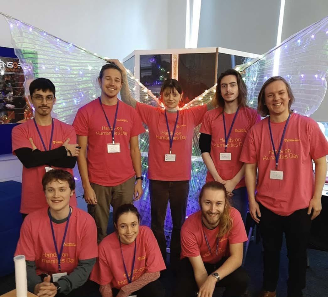
■ Demonstrator training and the delivery of workshops with the science-interested public at science festivals, including the Southampton Science and Engineering Festival and the hands-on optics workshop at the Arts and Humanities Festival;
■ A summer school for A-Level Physics pupils of Afro-Caribbean Heritage;
■ Disseminating good practice at national public engagement and outreach conferences.
This year the programme reached over 950 pupils, teachers and members of the public in face-toface activities, with a further 2,088 via on-line engagements, video views and podcast downloads. This was a 46 per cent increase in those reached in face-to-face activities from the previous year.
Virtualisation activities
Continuing the virtualisation project that began during the COVID-19 pandemic remained a focus of outreach this year. Photonics Explorer kits were provided to teachers free-of-charge, alongside a compulsory training session instructing them how to use these kits. This could potentially benefit 7,500 pupils in the next three years.
| Bringing photonics research to more diverse audiences
light-up
29 28
PhD outreach team demonstrating
their
wings
The virtual nature of the workshops meant that they achieved a wider geographic reach than physical workshops have previously done. Thirty teachers and two STEM Club managers attended the workshops which introduced teachers to using the equipment in the Photonics Explorer kit, such as lasers, LED units and polarisers. There was a 28 per cent increase in teachers’ knowledge of photonics after the workshops.
Student skills development
Fifteen students - both undergraduate and postgraduatewere provided with training this year. The sessions included an introduction to the Hub, the purpose of photonics outreach and public engagement, safeguarding training and basic science communication skills. This was followed by on-the-job training and ongoing self-reflection activities.
Activity delivery
The programme also delivered 21 face-to-face activities in 2022, including optics workshops at the Southampton Science and Engineering Festival (SOTSEF) and the Southampton Festival of Arts and Humanities. The workshops were designed to appeal to a wide agerange as well as family groups.
The workshop at the Southampton Festival of Arts and Humanities attracted almost 250 visitors. The activity ‘Play with Light’ featured two large demonstrations: a large

Pepper’s Ghost and Infinity Mirror, with two tables of fibre optics demonstrations – including fibre lamps, a telecommunications kit, and samples of fibres. Visitors were also able to participate in making kaleidoscopes and mobile phone Pepper’s ghosts. This workshop received a four out of five audience enjoyment rating, with 92 per cent of responses saying they would be ‘Likely’ or ‘Very likely’ to want to find out more about physics, having taken part in the workshop.
The postgraduate student demonstrators were asked to reflect on the event. They noted audience member’s responses were very positive about the activity: “What I learnt: people and young kids in general are a lot more enthusiastic about light and photonics than I would have thought.”
Working with an Arts Festival audience also enabled us to reach more women than traditionally found at a Science festival. With regards to the importance of diversity in photonics, Alice Iles, previously a PhD student who was involved with outreach activity said: “I am passionate about promoting women in STEM. This change won’t happen organically. Physics needs to be actively encouraged to schoolgirls and young women and there needs to be optical modules available to students in order to promote women’s engagement with photonics.”
Widening participation
Widening participation is an important aspect of outreach and public engagement. This year seven optics workshops were delivered to Year 8 pupils from underserved schools in order to expose them to photonics. These were delivered before pupils choose their GCSE options, a key point in children’s education as those who do not take Combined Science as a GCSE are very unlikely to take Physics at A-Level and follow a path that leads them to work in the field of photonics.
Pupils of Afro-Caribbean heritage were also invited to participate in a physics summer school. Pupils from Afro-Caribbean heritage face significant barriers to studying physics and so it is highly important to encourage diversity in photonics. They attended physics and astronomy talks, participated in practical activities and were given an introduction to the Hub by a postdoctoral researcher.
Disseminating best practice
The Hub outreach team shared their expertise this year, playing an active role in disseminating best practice to others involved in outreach and public engagement. Dr. Pearl John, Public Engagement Leader for the Hub, presented at the SEPnet Interact Conference in Cardiff with one of her postgraduate demonstrators. This conference is centred around encouraging best practice for outreach programmes in STEM.
“I was very happy to be able to share my experience of working with Afghan refugees during a workshop on light. The discussions we had thereafter were also helpful as they gave me lots of ideas on how to improve next time.”
With almost 200 attendees, the outreach team were able to share and reflect upon their experience of encouraging public engagement in photonics. Their chosen case study was the workshop they had held for Afghan refugee children in 2021, whereby they shared the strengths of the day and reflected on ways in which they would improve in the future.
Pearl was also interviewed on All Things Photonics a biweekly podcast produced by Photonics Media and she presented a live webinar chat for Electro Optics entitled: Communication and Outreach in Photonics.
| Bringing photonics research to more diverse audiences
31 30
Emilie Gerouville, PhD student, Optoelectronic Research Centre (ORC)
Images in University of Southampton’s £200m cleanroom complex Long-Term Optical Performance of Hollow-Core Fibres 34 Nonlinear Effects in Bent Large-Mode-Area Multimode Fibres 36 Integrated Silicon Photonic Circuits 38 Manufacturing of 2D materials 40 Directional VCSEL Lasers, and beam diffusers f or mobile phone face recognition systems 44 Development of Integrated Mid-Infrared photonic devices and systems 54 Development of Integrated Mid-Infrared Photonic Devices and Systems 48 Laser written scattering chip for spectral measurements 50 New Fibre Optic Components, Fibre Amplifiers and Lasers 52
33 32
Technology reports
Long-term Optical Performance of Hollow-Core Fibres
Challenge
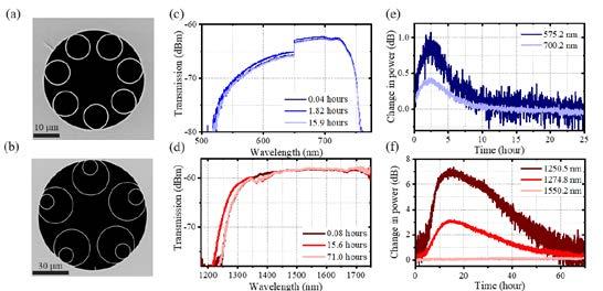
Hollow-core optical fibres (HCFs) enable low loss light transmission within a gasfilled core surrounded by a microstructured cladding. Two examples of HCFs fabricated at the University of Southampton are shown in Figures 1a and 1b. Due to light transmission in air, as opposed to in glass in conventional optical fibres, these specialty fibres offer a wide range of exciting properties including: low latency, low loss from ultraviolet to mid-infrared wavelengths, ultralow non-linearity and exceptional polarisation properties. The unique designs of these fibres, based on thin (~few hundred nanometre) silica membranes which define the core and cladding holes, mean that the long-term performance of HCFs may be impacted by different factors as compared to conventional fibres.
Our focus here is to assess the long-term optical and mechanical performance of HCFs in environments and configurations relevant to future deployment in various applications, and to develop techniques and fabrication processes to mitigate any reliability or aging effects observed.
Progress
We have been investigating how gas flow in and out of the holes within our HCFs can affect the optical properties of these novel fibres. This work is very important for accurate characterisation of HCFs as well as for the consistency of their longterm performance and builds on two important results that we have recently demonstrated.
Firstly, we have previously shown that immediately after fabrication, the gas pressure inside the core and cladding holes of an HCF is substantially below atmospheric pressure (~0.2 atm.) [1]. Therefore, if a HCF is exposed to atmospheric gas, for example in the lab during characterisation or later when installed in an application, gas from the surrounding environment will flow into the core and cladding holes due to the differential pressure. As the core and cladding holes have different crosssections (see Figure 1a), gas will flow into these regions at different rates; as the fibre core is larger, gas will fill into this region faster than the cladding holes. This creates a temporary pressure difference between the core and cladding regions.
One example of where this low initial pressure and subsequent pressure-driven gas flow is important is in combination with one of our further recent results, where we demonstrated that the transmission of an HCF can be significantly changed if the gas pressure inside the cladding holes is different to the gas pressure inside the fibre’s
Co-Investigator contact: Dr Natalie Wheeler nvw1v10@orc.soton.ac.uk

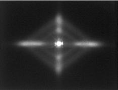
Figure 1: Scanning electron microscope images of (a) a tubular HCF and (b) a nested antiresonant nodeless fibre (NANF); (c) and (e) show the transmission as measured through the tubular HCF and NANF respectively at specific times after opening up the fibres to atmospheric pressure; (d) and (f) show the transmission over time for selected wavelengths for the tubular HCF and NANF respectively.
core [2]. This happens because the different gas pressures lead to slightly different refractive indices for the gases in the core and cladding, and even when the index difference is very small, this can still dramatically change the fibre’s optical properties.
To investigate this, we measured the transmission of two different types of HCF (see Figures 1a and 1b) over time, immediately after the core and cladding holes were exposed to atmospheric pressure. Figures 1c and 1d show the transmission over time as a function of wavelength, for three different times after opening up the fibres to atmospheric pressure. Overall, both fibres show a similar trend; straight after the fibres are exposed to atmospheric pressure, the transmission starts to increase, then after a certain time, this increase peaks and then the transmission decreases again to its initial level. This behaviour can be explained by the different filling times of the core and cladding holes [3]. Furthermore, we have shown that the magnitude of the transient change in transmission properties is dependent on the wavelength of the transmitted light; this is highlighted in Figures 1e and 1f where the transmission changes for selected wavelength are shown over time. Understanding of this transient behaviour and the timescales involved, along with the impact of fibre design and length, is very important for accurate fibre characterisation and stable performance in applications.
Future plans
The work described above is part of a larger on-going study into the performance of different HCF designs in a variety of different environmental conditions which are relevant to their deployment in a range of applications, including telecommunications.
References
[1] S. Rikimi et al, Journal of Lightwave Technology, 40(14), 4776-4785, 2022
[2] T. W. Kelly et al, Optica 8(6), 2021
[3] S. Rikimi et al, SPIE Photonics Europe 2022, Paper 12140-2
| High Performance Silica Optical Fibres | High Performance Silica Optical Fibres
35 34
Nonlinear Effects in Bent

Large-Mode-Area Multimode Fibres
Challenge
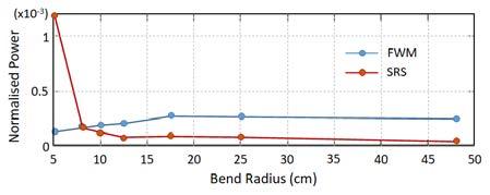
In material processing and manufacturing, multimode silica fibres are routinely utilised for high power, single-mode diffraction-limited laser delivery to the workpiece. As the power requirements and the distance to the workpiece increases, preserving the spectral characteristics and the beam quality of the delivered laser power with flexible, sliceable, high-power handling, solid core fibres, under real life, different coiling conditions becomes a great challenge. Nonlinear effects, such as Stimulated Raman Scattering (SRS) and Four-Wave Mixing (FWM), can increase the spectral content of the output beam and severely compromise the effectiveness of the optics in the processing head. In addition, bending induced modal distortion and intermodal FWM (IM-FWM) can transfer power to phase-matched higher order modes and decrease the output beam quality and beam stability.
Progress
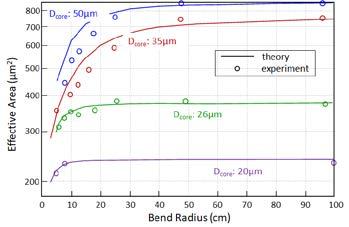
In this work, we launch the fundamental mode and study SRS and IM-FWM effects in large mode area (LMA), multimode (MM) fibres (core diameters: 20 μm-50 μm) under different bending radii (96cm-5cm) and a fixed length of 30m. Under bending, LMA fibres are known to suffer for severe modal distortion and effective area decrease. For the first time, we have used the increased SRS generation to infer the modal distortion and effective area decrease in bent fibres. It is shown that modal shrinkage increases with core diameter and bending curvature, in very good agreement with theory (see Figure 1).
The effective mode area decrease with bending increases the local intensity and it is expected to enhance nonlinear effects. Figure 2 shows the output signal, SRS (1st and 2nd Stokes) and FWM power variation with input peak power for a 50 μm core diameter fibre and bend diameters of 96cm and 10cm. It is shown that SRS is indeed increased as the bend diameter decreases from 96cm to 10cm. In contrast, the FWM power is decreased as the bend diameter decreases, despite the ~50% decrease in effective mode area (see Figure 1) and the expected doubling of the intensity. This is an unexpected result. In addition to intensity, IM-FWM is affected by the phase-matching of the participating modes and more work is required to understand the root cause of this dependence.
Figure 1: Fundamental mode effective area decrease with bending.
Figure 2: Output signal, SRS and FWM power variation with input peak power for different bend diameters (core diameter: 50μ m).
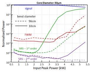
Figure 3 shows the normalised power variation of the SRS and FWM as a function of the bend radius for a fixed peak power of 5.5kW. It is shown that the IM-FWM is kept almost constant for bend radii down to ~17cm and progressively decreases thereafter, becoming smaller than SRS below a bend radius of ~7cm. This behaviour is currently under investigation.
Future Work
Experimental and theoretical work is under way to understand how the propagation characteristics of modes in LMA fibres depend on bending and how IM-FWM is affected by the phase-matching and overlaps of the participating modes. In addition to understanding beam delivery in MM fibres, this work is expected to shed light into the modal properties of high power fibre lasers, as well as their efficiency and stability.
| High Performance Silica Optical Fibres | High Performance Silica Optical Fibres
Co-Investigator contact: Professor Michalis Zervas mnz@soton.ac.uk
Figure 2
Figure 1
37 36
Figure 3
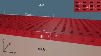
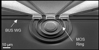
Integrated Silicon Photonic Circuits
Challenge
One of the key devices for telecom and datacom applications is an efficient optical modulator. We have implemented two approaches in our research: 1) realisation of an all-silicon optical modulator with small footprint and high speed operation, 2) deposition of materials that show superior modulation parameters compared to silicon and their integration with silicon. If broadband sources are used in absorption spectroscopy, we need devices that operate over a large spectral band. We have fabricated wide band waveguides and bends and also spectrometers with very good spectral resolution.
Progress
Ring optical modulators can have small size and power consumption. To fully utilise this potential, we have designed, fabricated and characterised a type of ring modulator known as a MOS Capacitor (MOSCAP) which accumulates carriers at an oxide barrier under a voltage bias, thereby changing the carrier density, and hence refractive index. In the process, we have identified an important mechanism for modulation enhancement which is unique to this type of modulator. Large absorption modulation that accompanies the phase modulation in the MOSCAP structure (see Figure 1) can be used to detune the coupling conditions of the ring resonator. This causes substantial changes in the resonance depth that can in turn enhance the intensity modulation as compared to that which results from shifting the resonance alone. Fabricated devices have demonstrated 20 dB of electro-absorption modulation at the resonance with a 3.5V bias change and a total modulation depth of 27 dB. These results have recently been accepted for publication in Nature Photonics.
PbZr x Ti1-xO3 (PZT) films have large Pockels coefficient and can potentially be used for efficient optical modulation. We have investigated growth of PZT on various substrates and have shown that defect-free films with very good crystallinity could be obtained on silicon if buffer layers are used. Various annealing temperatures have been applied and optimal conditions found. The next step is to implement such layers to demonstrate heterogeneous optical modulators in silicon.
We have already demonstrated wide band waveguides in silicon-on-insulator platforms (see Figure 2) with losses comparable to standard waveguides. The major issue was large bend loss, but we have recently demonstrated such waveguides with low bend loss. Simulated loss for a standard bend design was ~0.6 dB/90° for a radius of 300 μm. A new bend design, using fully-etched Euler bends, gives experimental loss of <0.2 dB/90° for a 20 μm radius thus significantly improving the performance. These bends will be used in a novel mid-IR Si spectrometer configuration, in which we have combined both analog and digital tuning of the interferometer arms and shown good spectral resolution.
Future plans
Future work will involve performance improvements of silicon near-IR and mid-IR devices and circuits, and will focus on: fabrication of more efficient optical modulators, integration of electronics, lasers and detectors, and realisation of spectrometers on chip.
|
Silicon Photonics
Figure 1: SEM image of the fabricated MOSCAP ring modulator.
| Silicon
Figure 2: Wideband waveguides with metamaterial cladding
Photonics
39 38
Co-Investigator contact: Professor Goran Mashanovich g.mashanovich@ soton.ac.uk
Manufacturing of 2D materials

Challenge
One of the greatest challenges the semiconductor industry faces is the replacement of current materials, as their physical limitations are expected to be reached during this decade [1]. 2D materials offer the ability to continue the scaling of devices offering reduced short-channel effects for transistors and excellent optical properties due to their atomically thin nature. This material family is predicted to be integrated in Morethan-Moore applications where processing and sensing take place at the same layer, in photonic integrated circuits as broadband photodetectors and electronic circuitry, but also in neuromorphic and quantum computing. There are three main challenges to overcome for the industrial uptake of these materials: Firstly, wafer-scale defectfree, uniform and independent control of layer number, stoichiometry and crystallinity. Secondly, the compatibility with existing processes such as silicon photonics and CMOS for co-integration. Thirdly, the absence of a performing p-type material for complementary integration. Our work aims to tackle all three issues by demonstrating significant improvements in electrical and optical properties along with improvements in the manufacturing processes, in particular wafer-scale deposition by introducing purpose-built equipment.
Progress
Following success in the demonstration of improvements in physical properties of 2D materials, efforts are now focused on advancing our manufacturing capabilities relevant to the commercial supply of these materials. Over the past years, we have developed a series of deposition protocols for 2D film growth to tune characteristics for different application specifications. In parallel we have been working on scaling these methods to larger wafer sizes from 4-inch to 8-inch. To evaluate and fully characterise our materials, in addition to our own device-oriented experiments, samples are provided to a broad range of industrial and academic collaborators from which we obtain valuable feedback on their performance.
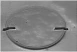
We have recently built a new 4-inch deposition system (see figure 1b) capable of growing 2D layers on 10 wafers in parallel with a layer non-uniformity of better than 4% across the entire wafer. This capability significantly increases the number of samples we can produce at one time, but also improves the compatibility of the samples with our collaborators’ post-processing equipment as it offers a more manufacturingrelevant form of the technology. To enable even larger wafer-scale depositions up to 8-inch, we have designed unique deposition equipment, in collaboration with local SME Thermic Edge Ltd. The equipment is designed to accommodate our most uniform large area process which is based on atomic layer deposition (ALD) to offer decoupled control of layer number, stoichiometry and crystallinity. The system offers a very robust solution as it has been meticulously designed and tested to withstand very corrosive environments (H2S) at temperatures up to 1200oC. We have now completed the build and are at the final testing and tuning phase, where we work on achieving the best possible control over the pressure, temperature, and gas delivery. A recent picture of the built equipment is shown in Figure 1a.
| Large-Scale
Manufacturing of Metamaterials and 2D Materials
| Large-Scale Manufacturing of Metamaterials and 2D Materials
Co-Investigator contact: Dr Ioannis Zeimpekis izk@soton.ac.uk
Figure 1a Figure 1b
41 40
Figure 1: 2D material deposition equipment. (a) 8-inch chamber and precursor distribution assembly. (b) 4-inch deposition system detail with wafer after deposition.
| Large-Scale Manufacturing of Metamaterials and 2D Materials
A wide range of large-scale 2D materials, including graphene, hexagonal boron nitride (hBN) and transition metal dichalcogenides (TDMCs) have been developed via chemical vapour deposition, Van der Waals epitaxy and atomic layer deposition. Examples of materials shared in the past year include 2D MoO3 to the University of Glasgow with whom we work to achieve p-type 2D layers by converting our material to MoTe2, to tackle one of the fundamental challenges of the technology. MoS2 and WS2 samples have been shared with Singapore University of Design and Technology to study the co-integration of 2D materials with phase change materials for tuning the properties of non-volatile photonic memories for integrated optoelectronics and free space photonics. We have worked closely with Sheffield to provide characterisation of epitaxially grown 2D layers for electronic and photonic applications material antimonene. Graphene samples have been exchanged with the National University of Malaysia and Northumberland University. We have supplied VdWE-grown TMDCs to the National Physical Laboratory to support our research on large area growth of 2D heterostructures [2]. We recently expanded our network of cross-departmental collaborators with work on energy storage electrodes made by integrating silicon nanowires and 2D MoS2 being undertaken with Electronics and Computer Science at the University of Southampton to fabricate large-area heterostructure samples. This material group has also sparked a new collaboration with Engineering at the University
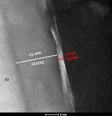
Large-Scale Manufacturing of Metamaterials and 2D Materials
of Southampton on electrodes for aluminium electrolyte batteries to overcome the limitations of lithium-ion batteries such as safety, availability and cost. Examples of these materials are illustrated in Figures 2 and 3. Expanding our involvement in green energy applications further, we were recently successful in a very competitive New Horizons EPSRC bid (EP/X016730/1), to demonstrate wearable thermoelectric energy harvesters using our large area 2D equipment.
Amongst our collaborators, our work with VTT Technical Research of Finland on the demonstration of ferroelectric field effect transistor memories has yielded excellent results [3] and we are now working on implementing our devices on a neural network to demonstrate efficiency in matrixvector multiplication operations for applications such as image recognition. Ongoing activities
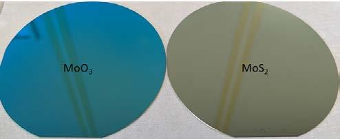
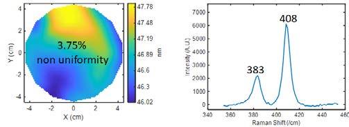
Figure 2: 2D material wafers produced using our home-built 4-inch multiwafer system. (a) An MoO3 and an MoS2 4-inch wafer. (b) Ellipsometry results showing a 3.75% worst case non-uniformity for a 4-inch MoS2 deposition. (c) Raman results verifying the quality of our MoS2 material.
supporting other research includes providing materials to three current EPSRC grants EPSRC EP/T014733/1, Fiberized Platforms for Integrated Nanosheet Materials, EPSRC EP/V040030/1, 3D Nanophotonics in Artificially Structured Chalcogenide Materials and EP/S036369/1, Composite Material Hollow-Core Fibres for Active Photonics.
Future Plans
We continue to work towards our objectives, bringing together our ongoing work developing new chemistry routes to 2D material synthesis and combining these with practical methods of depositing the materials at larger areas using deposition protocols at wafer scales compatible with modern semiconductor processes. Our aim is to expand these processes to our new 8-inch deposition equipment and achieve largearea control of the material properties while providing a complementary metal-oxidesemiconductor (CMOS) equivalent process compatible with CMOS back-end-of-theline, flexible, and photonic platforms. Achieving these goals will be a major step in the wider spread of this technology towards commercialisation which will enable future applications beyond what is possible with current materials.
References
[1] IRDS, Beyond CMOS, IEEE, 2021
[2] C-C Huang, et al. “Facilitating Uniform Large-Scale MoS2, WS2 Monolayers, and Their Heterostructures through van der Waals Epitaxy”, ACS Applied Materials & Interfaces 2022 14 (37), 42365-42373. DOI: 10.1021/acsami.2c12174
[3] Aspiotis N, et al. “Large-area synthesis of high electrical performance MoS2 by a commercially scalable atomic layer deposition process.” (Accepted in NPJ2D materials and applications) arXiv:2203.10309.
|
Figure 3: TEM image of a silicon nanowire coated uniformly with three layers of MoS2.
1b
Figure
a) Two 4 inch wafers
b) MoS wafer scan ellipsometry
43 42
c) MoS2 wafer Raman
Directional VCSEL Lasers, and beam diffusers for mobile phone face recognition systems

Challenge
3D vision and face recognition systems are now common in smartphones, but they utilise complex bulk optical systems that are very difficult and costly to assemble. Over the last two years, we have been working in conjunction with IQE plc (key supplier of laser epitaxy to Apple and Huawei) on the development of more compact replacement components for 3D face recognition systems for deployment in next-generation smartphones. This project exploits our granted Photonic Quasi-Crystal (PQC) patent portfolio which was recently purchased by IQE.
One of the key sub-modules is the infrared illuminator. This incorporates an array of very high-power VCSELS, along with a diffuser component to provide a specific illumination pattern.
VCSELs currently suffer from unavoidably large beam divergence angle (typically 60 0) requiring complex corrective optics, making the illuminator module bulky and expensive to assemble. They also require a complicated oxidation process that defines the laser aperture, and limits the power output.
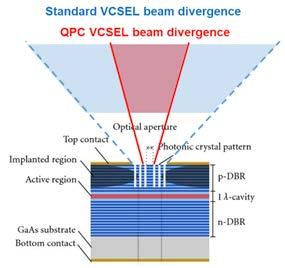
Our Photonic Crystal VCSEL technology solves the VCSEL beam divergence and power limitation problems, allowing control of the beam divergence angle direct from the chip dye without the need for external lenses (see figure 1a). It also allows very large circular MESAs to be used, making them suitable for very high-power LIDAR illumination, and high-speed telecoms applications.
Diffuser components are currently based on arrays of stalactite-shaped glass microlenses, typically 30 um in length, each with a unique length and curvature. These are incredibly difficult to manufacture, making the diffuser one of the most expensive subcomponents.
Utilising our legacy patents, we have devised a completely novel technological solution for the diffuser component, replacing the long glass stalactites with a sub-micron thick nano-patterned silicon layer.
concept..
(b) Photograph of laser beam projected onto a screen. PQC device has far smaller laser spot due to reduced beam angle.
of the VCSEL showing the oxidised layers. Central inset shows the full device, and where the cross-section images were.

| Large-Scale Manufacturing of Metamaterials and 2D Materials
| Large-Scale Manufacturing of Metamaterials and 2D Materials
Co-Investigator contact: Professor Martin Charlton mdc1@soton.ac.uk
Figure 1: (a) (Schematic cross-section of PQCVCSEL illustrating beam shaping
Laser beam projected onto screen Standard VCSEL Cross-section Circular device Epitaxial mirror layers Lateral oxidation distance QPC VCSEL – much smaller spot
Figure 2: FIB/SEM crosssection
45 44
Figure 1a Figure 1b
Progress
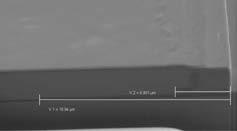
First sets of PQC-VCSEL devices demonstrated greatly reduced beam divergence (see figure 1b) and excellent electrical characteristics despite having very shallow holes and no aperture oxidation process step. Over the last year, the fabrication process has been scaled up to full 6in wafer process, and a 6in wafer-level aperture oxidation process developed to commercial standard (see figure 2). Next-generation devices, incorporating the new process and deeper holes, are expected to demonstrate extreme beam shaping, and high-power illumination.
PQC-diffuser components require the development of a reliable end-to-end manufacturing process from scratch. Over the last year, several new designs have been fabricated and tested, increasing optical efficiency to >96 per cent and achieving the required diffusion pattern (see figure 3), and specifications as required for current mobile phone systems. The key challenge was speeding up the electron beam lithography process used to define the complex nm scale pattern on glass to allow full 6in wafer patterning (see figure 4).
Working closely with IQE’s manufacturing teams in Taiwan, we are now in process of scaling up to mass-manufacture using cutting-edge nano-imprint lithography process and will commence production of customer demonstrator devices. A technology licencing agreement is currently under negotiation, and IQE plan to release a product based on the PQC-diffuser technology within the next 12 months.
| Large-Scale Manufacturing of Metamaterials and 2D Materials | Large-Scale Manufacturing of Metamaterials and 2D Materials
Figure 3: Example diffuser beam patterns projected onto a screen.
47 46
Figure 4: SEM image of nm scale pattern created by e-beam lithography.
Development of Integrated Mid-Infrared photonic


devices and
systems
Challenge
To demonstrate the integration of semiconductor devices such as lasers, LEDs and detectors on single chips for functional manipulation of mid-infrared light.
Progress
Our research in this platform is aimed at developing new manufacturing methods that will allow the integration of a range of photonics components, such as lasers, LEDs, detectors and quantum devices with passive semiconductor components such as waveguides, modulators and interferometers on silicon/Ge and InP platforms. The overall aim is to demonstrate new forms of integrated smart photonics chips such as integrated sensors, spectrometers, quantum processors and lab-on-chip diagnostic tools. The heterogeneous integration of different materials, devices and processes that in the past were often considered incompatible is now a major focus of the global development of smart electronic systems. But there remain many challenges in developing the manufacturing methods.
In this theme we have been continuing the development of two technological approaches to creating integrated photonic systems; with a focus towards on-chip integrated sensors with mid-infrared photonics. The University of Southampton has worked closely with the epitaxy and device teams in Sheffield to develop and evaluate new approaches to the problem, and have been working with industry and selected other academic groups to further the field.
We have made significant progress in the integration of Quantum Cascade Lasers (QCLs) on Si/Ge waveguide platforms with an iterative design approach now close to completion and testing in early 2023. We have in parallel developed a followon fabrication process involving industrial-level lithographic stepper equipment at Southampton. This tool will allow the entire process to be done on up to 8in Si/ Ge wafers and will eliminate the need for costly and time-consuming electron beam lithography systems to fabricate waveguide features. The work is expected to be completed in the next year and will demonstrate a full industrially-compatible manufacturing process for integrated mid-IR devices. The result of the work is of significant interest to our industrial partners and a stepping stone to commercial opportunities in the field of integrated sensors.
We have also made progress on the second approach to integrated mid-IR sensors, which is to develop homo-epitaxial integration of active components with waveguides on an InP semiconductor platform. The process involves epitaxial regrowth of semiconductor waveguides on InP. Whilst this is a standard process in the telecommunications industry, extending the wavelength into the mid-infrared means the overall dimensions of the waveguides and epitaxial regrowth are significantly increased and new means of achieving high quality epitaxial regrowth have been required. We have utilised a new MOVPE reactor commissioned in the National Epitaxy Facility in Sheffield to develop this work and the first measurement of InP-based waveguides at 3.3microns have been demonstrated in the last year. Further optimisation of the process will focus on compatibility with a number of industrial foundry services for InP and the demonstration of an industrially-compatible process for passive (waveguides) and active (lasers, detectors) components for integrated sensors.
(b) Deep UV scanner/ stepper system at the University of Sheffield which will be used for the demonstration of next generation of integrated mid-IR components on up to 8inch wafers.
| Integration
| Integration
Co-Investigator contact: Professor Jon Heffernan jon.heffernan@ sheffield.ac.uk
Figure 1: (a) Fabricated Si/Ge waveguides on a inch silicon substrate.
Figure 2: New MOVPE reactor installed in the National Epitaxy Facility in 2022. This reactor is being used to develop advanced epitaxial regrowth technologies including for mid-IR waveguides on InP.
Figure 3: Mid-infrared light at 3.3microns guided in an InGaAs/InP waveguide structure by MOVPE-based epitaxial regrowth.
Figure 1a
Figure 1b
Figure 2
49 48
Figure 3
Laser written scattering chip for spectral measurements
Challenge
To develop a compact low-cost optical spectrometer for metrology and optical sensing applications.

Progress
Optical spectrum characterisation is an important task in many areas of photonics, such as chemical analysis, metrology, and optical sensors. Typically, the spectrum is measured by simply breaking it down into individual spectral components using dispersion or diffraction. However, in order to achieve good spectral resolution, such a process requires a long optical path so that the spectral components are sufficiently well isolated. This problem can be effectively solved by using a scattering medium in which light of different wavelengths travels through a unique path to design a complex speckle pattern, which can be captured using conventional imaging sensors found on smartphones. Such an operating principle makes it possible to create a working spectrometer from just a few basic components: single mode fibre, scattering medium and camera.
Our group has developed a laser-written scattering chip in silica glass. Embedding scattering medium into silica substrate ensures good compatibility with silica fibres and provides outstanding long-term stability, which is important for successful exploitation of the technology. The scattering chip was evaluated as a solution for interrogation of optical systems, when the system needs to trace fine-resolution spectral responses linked to the sensed quantity (spectral shift induced by strain, bending, pressure, temperature etc.). Our team successfully demonstrated the use of scattering spectrometer for fibre Bragg grating interrogation. Conventional interrogation systems have to find a balance between resolution, cost and device size. A scattering chip-based system allows us to successfully address all aspects and offers high resolution in compact and low-cost packages. The high mechanical stability of the laser-written scattering chip allows us to measure strain applied to the fibre down to four micro strains. The interrogation system is configured to track speckle changes related to the applied strain effectively eliminating the need for additional data processing (finding Bragg wavelength peak shift, measuring peak bandwidth) required for conventional interrogators.
Future plans
The work will continue on integration of light source, driving board and scattering spectrometer onto a single ruggedised platform, which will allow us to carry out field tests in collaboration with our industrial and academic partners.
| Light Generation and Delivery
Figure 1: The image of scattering spectrometer. Single mode fibre delivers the light that is detected by the CMOS sensors mounted on the top of the spectrometer. Photo by Przemyslaw Falak.
| Light Generation and Delivery
51 50
Co-Investigator contact: Dr Martynas Beresna, M.Beresna@soton.ac.uk
New Fibre Optic Components, Fibre Amplifiers and Lasers
Challenge
Our research has focused on the development of new fibre optic components, optical fibre amplifiers and lasers in emerging new fibre types under development within the Future Photonics Manufacturing Hub.
Progress
Firstly, we have investigated wideband ytterbium-doped fibre amplifiers (YDFAs) suitable for potential future 1 μm telecommunication applications. Yb-doped fibre has a broad emission bandwidth extending from 976 nm to 1178 nm and has been widely used for high-power continuous wave or pulsed fibre laser development. However, there have been almost no reports of wideband YDFAs for data transmission since conventional silica fibres exhibit inherently high propagation loss around 1 μm (mainly from Rayleigh scattering). With the advent of new hollow-core fibre (HCF) designs (such as antiresonant fibres), the Rayleigh scattering loss in HCF can be much lower than achievable in solid silica fibres and a record low loss HCF operating around 1 μm (0.30 dB/km @1060 nm) has been successfully fabricated at the Optoelectronics Research Centre. This allows the consideration of 1 μm data transmission systems, thereby dictating the need for a suitable wideband YDFA. Note that 1 nm of spectral bandwidth at 1 μm is roughly equivalent to 2 nm of bandwidth at 1.5 μm in frequency terms/data carrying capacity and hence twice the data capacity/nm can be achieved simply by shifting the operational wavelength from 1.5 μm to 1 μm. Here, we have developed a wideband YDFA in a dual-stage configuration (similar to a gain-flattened erbium doped fibre amplifier (EDFA). An amplifier design enabling ~65 nm bandwidth (1025-1090 nm) was proposed through simulation and 50 nm bandwidth (1025-1075 nm) was realised experimentally (limited solely by the operating range of our gainflattening filter). The amplifier provides 20 dB average gain, <1 dB gain variation and <5.7 dB noise figure. Note that the 50 nm optical bandwidth of the gain-flattened YDFA is ~13.7 THz in the frequency domain, which is an almost 3.1 times increase in gain bandwidth compared to a C-band EDFA (~4.4 THz). In addition, the dual-stage YDFA (without a gain-flattening filter) has recently been used for 1 μm data transmission and we experimentally demonstrated 100-Gb/s transmission over a hollow-core fibre employing pulse amplitude modulation (PAM) -4 signals in the range 1020-1080 nm. While further improvements in the performance can be anticipated, our results clearly demonstrate the promising potential of data transmission in the 1 μm spectral region which may offer new opportunities for future optical transmission systems.
Secondly, we have demonstrated the controllable generation of picosecond (ps)-pulsed structured light from a coherently combined 6-core Yb-doped multicore fibre amplifier. With the spatial light modulator offering adaptive wavefront shaping and polarization control on the seed light to the multicore fibre amplifier, the complex amplitude of the amplified signal was fully controlled, enabling various spatial modes to be obtained in the far field. Linearly-polarized Gaussian beams, cylindrical vector beams, and linearly polarized 1st and 2nd order vortex beams were efficiently generated with high mode purity. The shaped beam has an average output power of 3-4W with a peak power of 10-14kW and a pulse duration of ~92 ps. The capability to flexibly generate various spatial modes with high peak powers should provide advantages in many applications in optical communication, laser material processing and biomedical imaging.
Thirdly, we demonstrated a high-energy and high-average power Mamyshev oscillator based on a high-performance step-index germanosilicate-cladding Yb-doped fibre. It is based on a self-phase modulation induced spectral broadening and offset spectral filtering approach to allow significant scaling of pulse energy. The laser directly generates a nearly diffraction-limited beam with an average power of 17W operating at the fundamental repetition rate of 14.01 MHz, corresponding to a pulse energy of 1.2 μ J. The pulses can be externally compressed to ~58 fs, leading to a peak power of ~13MW. To the best of our knowledge, this is the highest pulse energy with sub-100 fs duration ever obtained directly from a mode-locked fibre oscillator.
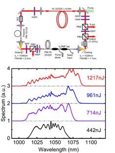
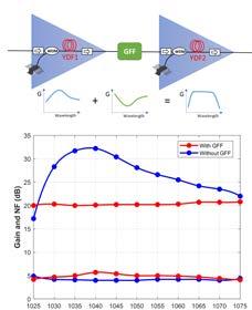
In addition, we have worked on optical interconnection between laser diodes and hollow-core fibres. Note that we have previously explored two HCF interconnection approaches (direct butt coupling and simple two-lens imaging) for coupling to a vertical-cavity surface-emitting laser operating at 850 nm and a very high coupling efficiency (~96%) was achieved from a two-lens system. Here, we have further extended our work to other wavelength bands with particular interest in visible/ultraviolet wavelengths and ~60-70% coupling efficiency has been successfully achieved. These wavelengths are particularly interesting because silica fibres are typically susceptible to solarization or high propagation loss within the fibre.
Future Plans
We will further optimise our fibre amplifiers/lasers to maximise the gain bandwidth and scale pulse energy and output power. Also, we will continue to work on direct interconnection between laser diodes and hollow core fibres in extended wavelength bands, with particular interest in the interconnection of mid-infrared quantum cascade lasers and visible/ untraviolet laser diodes to hollow-core fibres.

| Light Generation and Delivery
| Light Generation and Delivery
Co-Investigator contact: Dr Yongmin Jung ymj@orc.soton.ac.uk
Figure 1: Figure 1: Wideband gainflattened ytterbium-doped fibre amplifier for 1 μ m data transmission.
53 52
Figure 2: High-energy, high-power Mamyshev oscillator
Deputy Director and Manager: Professor Gilberto Brambilla, University of Southampton

Co-Investigator: Professor Martin Charlton, University of Southampton

Project Administrator: Liz Gilbride, University of Southampton

Deputy Director: Professor Jon Heffernan, University of Sheffield

Co-Investigator: Professor Dan Hewak, University of Southampton

Public Engagement Leader: Pearl John, University of Southampton
Event Coordinator: Emma Keeley, University of Southampton
Business Development Manager: Amir Kayani, University of Southampton

Industrial Liaison Manager: Dr John Lincoln
Co-Investigator: Professor Goran Mashanovich, University of Southampton

Business Development Office: Sarah Martin, University of Southampton
Research and Relationship
PR Officer: Michelle Mitchell, University of Southampton
Principle Investigator and Director: Professor Sir David Payne, University of Southampton


Co-Investigator: Professor Francesco Poletti, University of Southampton
Co-Investigator: Professor Graham Reed, University of Southampton
Co-Investigator: Professor David Richardson, University of Southampton

Co-Investigator: Professor Jayanta Sahu, University of Southampton

Co-Investigator: Dr Natalie Wheeler, University of Southampton


Co-Investigator: Professor Michalis Zervas, University of Southampton

Co-Investigator: Professor Nikolay Zheludev, University of Southampton

With special thanks to:
Carbon Trust, Huawei, Honeywell Aerospace, II-VI Photonics, IQE, IS Instruments, Lightpoint Medical, Lumenisity, Merck, Microsoft, NorthLab Photonics, Northrop Grumman, Oclaro, Phoenix Photonics, PragmatIC Printing, QinetiQ, Rockley Photonics, Seagate Ireland, Sestosensor, SPI Lasers, Breakthrough Prize, Defence Science and Technology Laboratory (DSTL), European Office of Aerospace Research & Development, Engineering and Physical Sciences Research Council (EPSRC), European Commission, Horizon 2020, Innovate UK, Royal Academy of Engineering, Royal Society
| The team
55 54

If you’d like to know more about the Future Photonics Hub, or find out how we can work together, please contact us: +44 (0)23 8059 9536 contact@photonicshubuk.org www.photonicshubuk.org Follow us @PhotonicsHub
