27 minute read
Technology reports
Next Article

Long-Term Optical Performance of Hollow-Core Fibres 42
Advanced Beam Shaping in High Power Fibre Lasers 45
Developing Large Mode Area Fibres for High-Energy and High-Average Power Laser Systems 47
Active Silicon Photonic Devices for the Mid-Infrared 48
Optical Components for 3D Vision Systems 50
Advanced Metamaterial Nanostructures 52
Manufacturing and Application of 2D Materials 54
Development of Integrated Mid-Infrared On-Chip Photonics 56
Novel Forms of Interconnection and Device Integration for Emerging Multicore, Multimode and Hollow-Core Fibres 58
Progress on Active and Hollow-Core Fibres Based on Non-Silica Glasses 60 Images in University of Southampton’s £200m cleanroom complex
| High Performance Silica Optical Fibres
Long-term Optical Performance of Hollow-Core Fibres
Challenge
To assess the long-term optical and mechanical performance of hollow-core fibres (HCFs) in environments and configurations relevant to future deployment in various applications. To develop techniques and fabrication processes to mitigate any reliability or aging effects observed.
Progress
The unique combination of optical properties offered by HCFs, such as ultralow latency, low non-linearity and wide transmission bandwidth, derive from guidance of light within an air-filled or hollow core. Yet, the microstructure that defines the hollow core presents a unique geometry, including very thin, curved glass membranes and the holes within the microstructure which usually contain gas content throughout the entire fibre length. The impact of this geometry on the long-term performance of these fibres is currently largely unexplored. We are investigating various effects related to the gas content within the fibre and the interaction of these gas species with the glass surfaces within the fibres.
Co-Investigator contact:
Dr Natalie Wheeler nvw1v10@orc.soton.ac.uk
Firstly, we have examined the initial internal conditions of a HCF immediately after fabrication, including internal gas composition and pressure. To do this, we seal the ends of the HCF straight after the fibre has been drawn, in order to preserve the initial conditions. Then via absorption and Raman spectroscopy, we have monitored the change in gas composition and pressure as a function of time, after the fibre ends are opened up to atmosphere. In this work, we have compared experimental measurements with gas flow simulations and identified that the pressure inside a HCF immediately after fabrication is substantially below atmospheric pressure; this has important implications for HCF storage and handling post-fabrication. | High Performance Silica Optical Fibres
Furthermore, we have investigated the optical performance of HCFs in two scenarios: (i) where the fibre is spliced at both ends to standard, all-solid optical fibre (effectively hermetically sealing the gas content within the core and cladding holes that run along the fibre length) and (ii) where light is free-space coupled into the fibre and therefore the gas within the fibre can exchange with the surrounding atmosphere, at a rate depending on the initial fibre conditions and the environment.
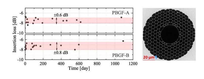
Figure 1: Transmission of two HC-PBGFs (PBGF-A, cross-section shown left) as a function of time. Both HCFs have been spliced at both ends to conventional, all-solid fibre; this provides low loss optical coupling but also hermetically seals the gas content present in the core and cladding holes inside the fibre.
In the spliced condition, we have monitored the transmission of several HCFs over time. Figure 1 shows the transmission of two hollow core photonic bandgap fibres (HC-PBGFs); this has been periodically monitored over more than 2 years and, within experimental uncertainty, the transmission of the fibres has remained consistent. This is very promising for data transmission applications where this deployment scenario is relevant.
| High Performance Silica Optical Fibres
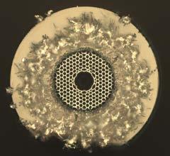
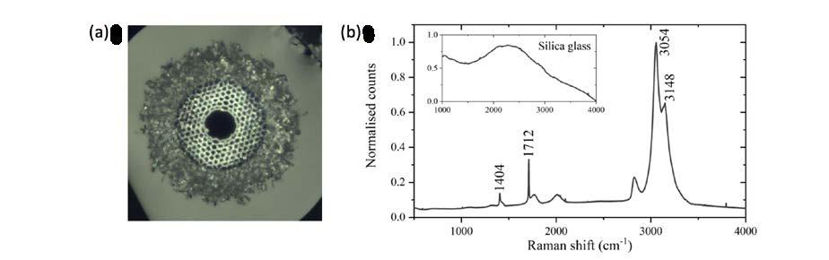
Figure 2: (a) Optical microscope image of a F300 HC-PBGF, where contamination is clear after 1 day; (b) Raman spectroscopy of silica glass (inset) and contamination. The Raman spectrum of the contamination agrees very well with reference spectra for ammonium chloride.
In the free-space coupling scenario we have studied end-face degradation for different HCF geometries and for HCFs fabricated from different grades of high purity silica (the starting point for HCF fabrication). HCFs made from F300 (high chlorine content) glass are known to have issues of contamination ‘growing’ from fibre end-faces post-cleaving; this is a particular issue in free-space experiments where the contamination reduces coupling efficiency into the HCF over time. Figure 2(a) shows a F300 HC-PBGF where the end-face has been cleaved and left for 1 day; significant contamination is present. Figure 2(b) compares the Raman spectrum of silica glass with the Raman signal of the end-face contamination; from these measurements we identified the contamination as ammonium chloride. In further work we have identified the likely sources of the ammonium chloride and means to remove it, this includes using a different grade of silica glass as a starting material. We have fabricated HC-PBGFs from F320 silica glass which, 50 days after cleaving, are substantially contamination-free.
Future plans: In ongoing work, we are investigating the optical performance of HCFs as a function of time in free-space conditions. We are studying various fibre designs (both HC-PBGFs and anti-resonant fibres) fabricated from different glasses. We are also investigating the gas composition within HCFs as a function of time and the impact of this on fibre aging. | High Performance Silica Optical Fibres
Advanced Beam Shaping in High Power Fibre Lasers
Co-Investigator contact:
Professor Michalis Zervas mnz@soton.ac.uk
Figure 1a
Figure 1b Challenge
With the forthcoming digital manufacturing and industry 4.0 upon us, a new generation of “smart” fibre laser is required, offering increased flexibility and controllability to respond to the new emerging challenges. For example, it is recognised that the ability to “structure” and shape the output beam profile of a laser can potentially yield significant improvements in speed, efficiency, and quality over conventional lasers, in processes such as laser cutting, welding, and additive manufacturing. Fibre lasers (FLs) significantly outperform all other competing technologies offering record output powers and beam qualities, ranging from single-mode (SM) 10kW, with beam quality factor M2~1.1, to highly multimode (MM) outputs of 100kW with M2~30. Due to their excellent waveguiding properties, FLs offer the possibility to uniquely structure the laser output beams and extend their applicability. The challenge is to develop novel all-fibre technologies in order to provide advanced beam shaping in high power fibre lasers (HPFLs) and evaluate their impact on material processing.
Progress
In our research, we have developed a novel all-fibre beam shaping technology, which relies on specially designed, in-fibre, adjustable mode couplers, and it is scalable to multi-kW levels. In contrast with other existing commercial solutions, our unique approach provides extensive mode-shape variability, from true fundamental mode to more complex higher-order azimuthal modes through multimode (MM) delivery fibres. Figure 1(a) shows the schematic of a special infibre beam shaper acting upon the single-mode (SM) Gaussian-like (LP01) output of a HPFL and transforming it into a complex multipetal (LP41) beam supported by the MM delivery fibre. The multipetal beam is stable and extremely robust against severe external perturbations, as required by industrial material processing systems. Our special in-fibre beam shaper can be set to provide a range of structured multi-petal ring-like beams (LP31 – LP61) of varying complexity and beam-quality factor (M2), as shown in Figure 1(b).
| High Performance Silica Optical Fibres
The beam shaping technology has been transferred to SPI Lasers Ltd and has been commercialised under the trademark variMODETM. The impact of the different beam shapes achieved with the variMODETM technology has been studied in cutting and welding stainless steel (SS), aluminium (Al) and mild steel (MS). In the case of MS cutting, ring-like beams reduce the power requirements by ~25% to achieve the same result with standard Gaussianlike beams. Significant improvements have also been observed in welding applications. Figure 2 shows an example of keyhole welding cross-sections achieved by a standard Gaussian-like (LP01) beam and a structured multipetal beam (LP61). The laser output power was 1.6kW and the focused beam spot-size 400μm. Such structured-light multi-petal beams are produced and used in industrial applications for the first time. It is shown that the use the novel multi-petal beams result in a superior welding, uniform along the entire depth.
Future work
The preliminary cutting and welding superior results were unexpected and efforts are now made to understand better the underlying light-matter interactions and define optimum beam shapes for ultimate welding and cutting performance. In addition, new beam-shaping technologies and novel configurations will be studied in order to increase the beam-shaping speed by one to two orders of magnitude, from the current ms to tens of μs regime. This will enable even faster material processing speeds, and extend the material processing capabilities of the new generation of “smart” fibre lasers, with truly programmable beam-shaping capabilities.
Figure 2
| High Performance Silica Optical Fibres
Developing Large Mode Area Fibres for High-Energy and High-Average Power Laser Systems
Challenge
Modified chemical vapour deposition (MCVD)-solution doped technique is widely used in today’s manufacturing of rare-earth (RE) doped silica optical fibre preforms. However this technology has its limitations when it comes to increasing the volume of doped material, attaining a homogenous doping at high doping levels of REs and codopants, and fibres with tailored dopants and refractive index profiles. Advances in doped fibre fabrication techniques to overcome these limitations are in demand for the next generation of active optical fibres that will take high power laser technology to its next level.
Co-Investigator contact:
Professor Jayanta Sahu jks@orc.soton.ac.uk
Progress
Our research has focused on developing an industry compatible MCVD-gas phase based RE-doped fibre preform fabrication technique that is suitable for realising multi-layered preforms with complex RE doping profiles. In addition, the fabrication technique allows a rapid production of preforms with a large doped core volume compared to the conventional MCVD-solution doping process.
The work has concentrated on optimisation of deposition parameters and core glass compositions for RE-doped (i.e., Yb3+, Er3+ and Tm3+) silica fibres, suitable for efficient high power laser operations at 1 μm, 1.55 μm, and 2 μm wavelength regions. Figure 1 shows the MCVD-gas phase process, where deposition of a transparent RE-doped phosphosilicate (PS) layer inside a silica glass substrate tube is presented. It is worth noting that PS is a preferred choice of host material for Yb3+ to suppress the photodarkening effect in high power lasers. However, RE-PS fibres are generally considered difficult to fabricate due to evaporation of P2O5 during the preform fabrication process, resulting in a central dip in the core refractive index profile that has detrimental effect on the output beam quality of fibre lasers. Our preform fabrication process has been optimised to minimise the central-dip in RE-PS fibres. Figure 1: A snap shot of the RE-doped preform fabrication process using an MCVD-gas phase technique. The green emission is an indicator of Er content in the preform
| Silicon Photonics
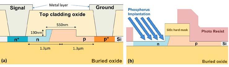
Active Silicon Photonic Devices for the Mid-Infrared
Co-Investigator contact:
Professor Goran Mashanovich g.mashanovich@soton. ac.uk
Challenge
The mid-infrared (mid-IR) spectral region is of interest for applications in gas, chemical and biomedical sensing, as well as in communications. We have focused on tackling two key research challenges to enable the realisation of inexpensive mid-IR optical systems. These challenges are: realising room temperature detectors based on suspended silicon waveguides and fabricating mid-IR optical modulators in silicon.
Progress
One of the most important devices for silicon mid-IR circuits is an integrated detector, which should ideally work at room temperature. We have been working on realising such a device based on our suspended Si technology. In the frame of this project, we have already demonstrated a library of robust suspended silicon devices for wavelengths up to 8 micrometers. This suspended platform is now being adapted for use as a multi-project wafer to enable multiple researchers in the UK and worldwide to access the platform through the EPSRC-funded CORNERSTONE foundry project.
The detector is shown in Figure 1 and comprises a suspended Si waveguide with a subwavelength lateral cladding, an antenna absorber on top of the waveguide core, an amorphous silicon (a-Si) bridge and two contacts. Due to the absorption of mid-IR light, enhanced by the presence of the antenna, the temperature of the a-Si bridge increases thus changing the bridge resistance which results in a change of the current between the two metal contacts. We have recently demonstrated this detector at a wavelength of 3.8 μm with a sensitivity of 24.62 %/mW, improving our previous results by more than one order of magnitude. | Silicon Photonics
Figure 1: Schematic of a room temperature midIR detector based on waveguide-integrated microbolometer
The second focus was on performance improvements of mid-IR silicon optical modulators for the 2 μm band. The modulators were based on carrier depletion (Figure. 2(a)) and were fabricated by the self-aligned process (Figure. 2(b). Fabricated MachZehnder and Michelson interferometer based silicon-on-insulator optical modulators were characterised using both OOK and PAM-4 schemes and showed world leading daterates of 25Gb/s with extinction ratios in excess of 6dB.
Figure 2: (a) The phase shifter cross section of the 2 μm MZI/MI modulator. (b) Self-aligned process used in the fabrication.
Future work
Future work will involve performance improvements of silicon mid-IR devices, such as larger sensitivity of detectors, demonstration of detection at longer wavelengths, fabrication of more efficient optical modulators and realisation of frequency combs based on such modulators, and integration of mid-IR sources and silicon and germanium mid-IR circuits.
| Large-Scale Manufacturing of Metamaterials and 2D Materials
Optical Components for 3D Vision Systems
Challenge
3D vision and face recognition systems are now common in smart-phones, but they utilise complex bulk optical systems that are very difficult and costly to assemble. Over the last 2 years we have been working in conjunction with IQE plc (key supplier of laser epitaxy to companies such as Apple) on developing more compact replacement components for 3D face recognition systems for deployment in next generation smartphones. This project exploits our granted Photonic Quasi-Crystal patent portfolio which was recently purchased by IQE.
One of the key sub-modules is the infra-red illuminator. This incorporates an array of very high power VCSELS, along with a diffuser component to provide a specific illumination pattern. VCSELs currently suffer from unavoidably large beam divergence angle (60 degs typically) requiring complex external corrective optics, making the illuminator module bulky and expensive to assemble. They also require a complicated oxidation process that defines the laser aperture, and limits the power output.
Our Photonic Crystal VCSEL technology solves the VCSEL beam divergence and power limitation problems, allowing control of the beam divergence angle direct from the chip dye without the need for external lenses. It also eradicates the oxidation step entirely, greatly simplifying-mass manufacture and allowing larger higher power lasers to be produced.
Co-Investigator contact:
Professor Martin Charlton mdc1@soton.ac.uk
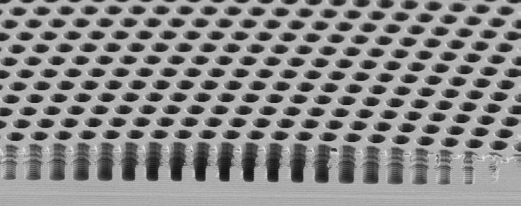
Figure 1: Photonic QuasiCrystal pattern etched in GaAs epitaxy. | Large-Scale Manufacturing of Metamaterials and 2D Materials
Diffuser components are currently based on arrays of stalactite shaped glass micro-lenses, typically 30 μm in length, each with a unique length and curvature. These are incredibly difficult to manufacture making the diffuser one of the most expensive sub-components.
Figure 2 left: Optical microscope image of completed PQC-VCSELs, right: SEM of PQC-VCSEL surface. Utilising our legacy patents we have devised a completely novel technological solution for the diffuser component, replacing the long glass stalactites with a sub-micron thick nano-patterned silicon layer.
Progress
Work on PQC-VCSELS resulted in a robust wafer scale fabrication process flow, and a novel etch processes for the Photonic Crystal pattern (Figure 1). Several batches of PQC-VCSEL devices were fabricated (Figure 2), demonstrating greatly reduced beam divergence whilst maintaining excellent electrical characteristics under test (Figure 3). Most significant, these prototypes proved that the oxidation process could be eliminated entirely and that arbitrary power scaling was indeed possible meaning arrays of VCSELs currently used in face recognition systems could be replaced by just a few large diameter PQC-VCSELS.
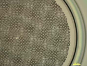
Figure 3: PQC-VCSEL array under test. Work on the PQC-diffuser component required the development of a reliable end to end manufacture process from scratch. The key challenge was development of a high fidelity, large area, electron beam lithography process to define the complex nm scale pattern on glass, pushing our e-beam system to its limits. 6 generations of PQC-diffuser prototypes were designed and fabricated. Optical tests showed the latest batch met real-world customer specifications as required for current mobile phone systems.
IQE plan to release a product based on the PQC-diffuser technology within the next 12 months and a technology licensing agreement is currently under negotiation. Our focus has now shifted to solving mass-manufacturing challenges, working closely with IQE’s manufacturing teams in Taiwan.
| Large-Scale Manufacturing of Metamaterials and 2D Materials
Advanced Metamaterial Nanostructures
Challenge
We manufacture reconfigurable photonic metamaterials based on dielectric membranes of nanoscale thickness that are nanostructured by focused ion beam milling to create periodic structures with moving parts. Due to their subwavelength unit cell size, such reconfigurable structures are effective optical materials, with optical properties controlled by temperature, electric field, magnetic field or even light.
Progress
Figure 1 shows one of our recent breakthroughs. This nanomechanical metamaterial exhibits giant electrogyration, i.e. dependence of optical activity on electric field. While the effect has been known in dielectrics, semiconductors and ferroelectrics since the 1960s, it is vanishingly small in natural materials. Here, we engineered a metamaterial were electrogyration is a million times stronger, achieving more than 10° polarisation rotation in a layer of 100s of nm thickness in response to a few volts. Electric field deforms every second nanowire of the structure. Upon deformation the structure becomes different from its mirror image, i.e. chiral, and starts to rotate the polarisation of light. The observation of giant electrogyration turns this phenomenon into a functional part of the electro-optic toolkit with application potential.
Co-Investigator contact:
Professor Nikolay Zheludev niz@orc.soton.ac.uk
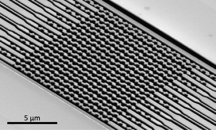
Figure 1: Electrogyration in metamaterials: Chirality and polarization rotatory power that depend on applied electric field. | Large-Scale Manufacturing of Metamaterials and 2D Materials
In related work, we have introduced a new technique for detecting and imaging movements with picometre (sub-atomic) displacement sensitivity, which can be deployed on a majority of existing scanning electron microscopes.
Nanoscale objects move fast, oscillating at kHz-MHz frequencies, and such movements (thermal or externally driven) underpin the functionality of numerous micro/nano-opto/ electro-mechanical (meta)materials, devices, sensors and systems. However, there are currently no routinely available techniques for quantifying and mapping such movements.
Our approach is based on real-time spectral analysis of variations in secondary electron emission from moving objects interrogated with a focused electron beam. It is sensitive to displacements at sharp, high-contrast edges of an object and has a typical noise level of order 1 pm/Hz1/2, thus allowing for the study of movements with sub-atomic amplitudes (the radii of isolated neutral atoms range between 30 and 300 pm).
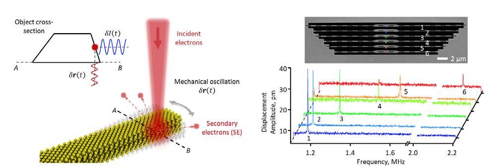
Figure 2: Detection of sub-atomic movement in nanostructures.
We have demonstrated applications to the measurement of natural frequencies and displacement amplitudes of thermal motion; hyperspectral visualisation of driven oscillation modes in nano-cantilevers and more complex, technologically-relevant (MEMS and reconfigurable photonic metamaterial) device structures.
| Large-Scale Manufacturing of Metamaterials and 2D Materials
Manufacturing and Application of 2D Materials
Challenge
To achieve CMOS compatible, wafer scale processing of 2D materials for optoelectronics applications, demonstrating an order of magnitude improvement in electrical characteristics.
Progress
During 2020, our research has continued to focus on optimising the electrical properties of uniform, wafer scale, atomically thin 2D films for use in next generation transistor devices and large areas transition metal di-chalcogenide monolayers for a variety of emerging electronic and photonics applications.
Co-Investigator contact:
Professor Dan Hewak dh@orc.soton.ac.uk
In collaborative work with Brazil, China and the University of Nottingham here in the UK, we have found that ionising radiation (gamma ray) interacts strongly with twodimensional WS2 which induces effective p-doping in the samples. As the radiation dose increases, the p-doping concentration increases substantially. These results, published in May in the journal Nanoscale Horizons, have shown that a detector based on monolayer WS2 is an appealing candidate for sensing high-energy photons at small radiation doses.
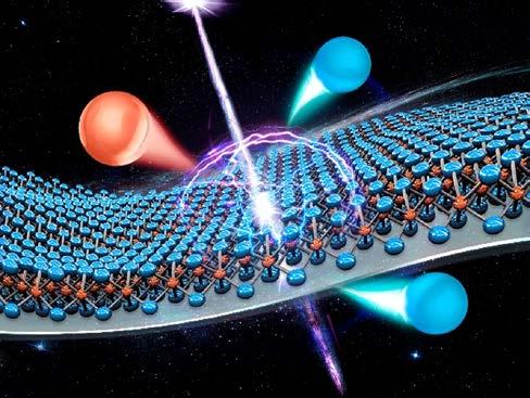
Figure 1: shows A conceptualised drawing of a γ-ray interaction with a WS2 monolayer illustrating the generation of secondary γ photons (in the silicon substrate), electron/hole pairs, fast electrons, and creation of S and W vacancies in the monolayer. | Large-Scale Manufacturing of Metamaterials and 2D Materials
Device performance continues to improve as our current generation of FET transistors molybdenum disulphide (MoS2), as shown in Figure 2, improve in performance through modifications in the fabrication methodology, in particular, optimisation of the annealing conditions post deposition. Statistical evaluation of devices fabricated, as shown in Figure 3.
Integration plays an important role in our research and to this end we have developed a large scale transfer process to facilitate their integration with a wide range of flexible optoelectronics, silicon photonics, optical fibre and III-V devices.
Future work
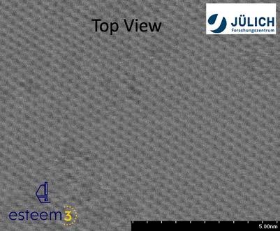
Figure 2: Scanning tunnelling microscope (STEM) image (top view) of MoS2 showing individual atoms of molybdenum (Mo) in a two dimensional crystalline lattice. Image taken by Forschungszentrum Jülich (Germany) through funding provided through ESTEEM3.
Figure 3: Histogram showing the improvement in device mobility in current devices compared to the first generation of devics fabricated. We continue to collaborate with industrial partners who are providing valuable target specifications for electrical performance. Most exciting for the team is our work commencing 2021 on the design and fabrication of an 8 inch (200 mm) capability for wafer scale processing up to 1200oC under inert or reactive gas conditions. This will be a major step forward in bringing wider spread commercialisation of 2D materials.
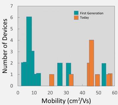
Figure 3
| Integration
Development of Integrated Mid-Infrared On-Chip Photonics
Challenge
To demonstrate the integration of semiconductor devices such as lasers, LEDs and detectors on single chips for functional manipulation of Mid-Infrared light.
Progress
Our research in this platform is aimed at developing new manufacturing methods that will allow the integration of a range of photonics components, such as lasers, LEDs and detectors with passive semiconductor components such as waveguides, modulators and interferometers on GaAs, silicon or silicon/Ge platforms. The overall aim is to demonstrate new forms of integrated smart photonics chips such as integrated sensors, spectrometers, quantum processors and lab-on chip diagnostic tools. The heterogeneous integration of different materials, devices and process that in the past were often considered incompatible is now a major focus of the global development of smart electronic systems. But there remain many challenges in developing the manufacturing methods.
In this theme we have been continuing the development of two technological approaches to the problem of creating integrated photonic systems; with a focus towards on-chip integrated sensors with mid-infrared photonics. The University of Southampton has worked closely with the epitaxy and device team in Sheffield to develop and evaluate new approaches to the problem, and have been working with industry and selected other academic groups to further the field.
Co-Investigator contact:
Professor Jon Heffernan jon.heffernan@sheffield.ac.uk
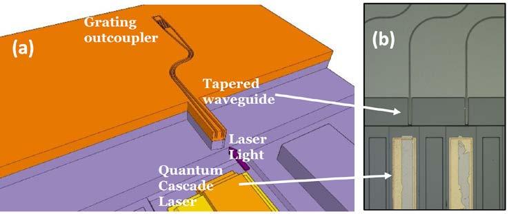
Figure 1: (a) Schematic of flip-chip integration of InPbased Quantum cascade laser (QCL) with a Si/Ge waveguide structure. (b) Microscope image of flip-chipped devices | Integration
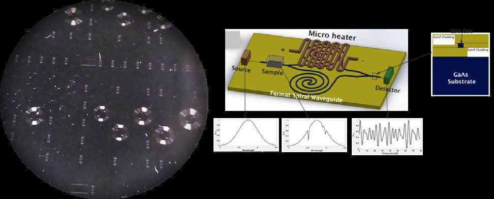
Figure 1: Schematic of on-chip FTIR spectrometer on a GaAs chip. On the left is the fabricated wafer including spiral waveguides.
We have continued work on hybrid photonic technologies using Quantum Cascade lasers epitaxially grown on Indium Phosphide substrates in Sheffield.
Lasers with excellent performance characteristics at an emission wavelength of 5.6μm have been developed and this wavelength is suitable for detection of important industrial gases such as Ammonia. The lasers have been ‘flip-chipped’ to integrate with photonic chip technology based on Silicon/Germanium substrates which were prefabricated at the University of Southampton (Figure 1). The flip-chip of large structures such as QCLs has required a significant development of the semiconductor processing technology to ensure that optical coupling of the laser with the Silicon/Germanium waveguides is optimum. High coupling efficiency and low loss of light is critical to integration technology as it has a direct impact on sensitive and ultimately on cost.
With a focus on manufacturing efficiency and cost we are also investigating a second approach to creating integrated on-chip sensors. This is based on homogenous integration of different photonic components onto a single III-V semiconductor substrate. We are aiming to demonstrate an on-chip Fourier Transform Interferometer (FTIR) for spectral analysis on a GaAs platform. A schematic of the structures is shown in Figure 2 and the principle is based on an on-chip Max Zender interferometer with thermally tuneable waveguides. The development of this technology for the mid-IR spectral region is a new area of research. To achieve mid-IR waveguiding we have developed a buried waveguide approach using epitaxial regrowth by MOVPE at the University of Sheffield. GaAs waveguides are buried in a cladding of GaInP which is lattice matched to GaAs and ensures high optical and structural integrity of the material. Because of the mid-infrared target wavelength of around 4 microns, the GaInP clad region has to be very thick (>5 microns) and this requires significant development of the epitaxial regrowth. Following initial demonstration of good buried waveguides, we have now started to optimise the process to obtain the lowest loss structures. In particular, because we use spiral waveguides (Figure 2.) we have investigated the effect of crystal orientation on the regrowth process. Initial investigations using both physical and optical characterisations of the waveguides show limited impact of waveguide orientation, but further research is required leading to potentially new designs.
| Integration
Novel Forms of Interconnection and Device Integration for Emerging Multicore, Multimode and Hollow-Core Fibres
Challenge
To develop novel means of interconnecting emerging new fibre types under development within the Photonics Manufacturing Hub to other fibres and/or to other functional components.
Progress
Our research this year has focused on the development of industrial grade interconnection and integration platforms enabling ready integration of these novel fibres into devices and sub-systems.
Firstly, using micro-optic collimator technology, we have developed various inline fibre components based on few mode fibres, multicore fibres and hollow-core fibres. This includes components such as isolators, circulators, 2x2 fibre couplers, gain-flattening filters and WDM couplers, which we now routinely fabricate in-house in support of our wider research goals. We can even produce hybrid fibre components incorporating multiple optical functions (e.g. an isolator + WDM coupler). Note that these novel optical components have subsequently been used in the construction of compact few mode (or multicore) fibre amplifiers and amplifier modules, which have successfully been made in both core-pumped and cladding-pumped configurations. Significantly, we have received several consultancies form one of our industrial Hub partners for the supply of few mode and/or multicore fibre components and optical amplifier assemblies. Various prototype devices have now been supplied for real world testing/ applications. More recently, we have built few-mode multicore fibre amplifiers (e.g. 7-cores x 6-modes) operating in both the C-band and L-bands and shipped them to NTT Laboratories in Japan, where our collaborators have successfully tested and used them in various data transmission experiments.
Co-Investigator contact:
Professor David Richardson, djr@orc.soton.ac.uk | Integration
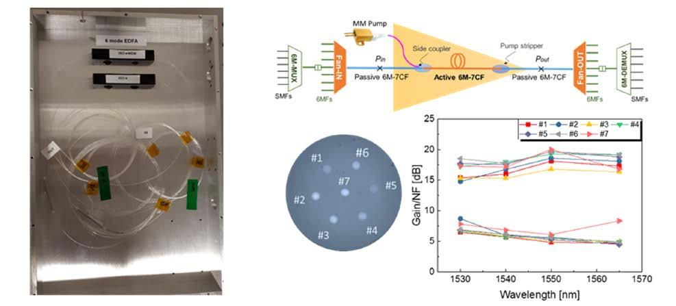
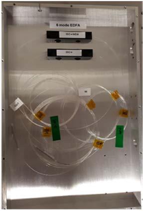
Figure 1 left: Fully integrated 6-mode EDFA module
Right: 6-mode 7-core fibre amplifier We have also worked to integrate metamaterial samples into multicore fibres. In particular, we have developed a 7-core fibre device incorporating meta-surfaces on each core for polarisation analysis and fabricated associated fan-in/fan-out devices to access individual cores.
In addition, we have collaborated with researchers at the University of Bath on the topic of logarithmic index profile fibre, leading to fibre tapers with invariant mode field diameter along their length and enabling adiabatic mode transitions for all spatial modes (not just for the fundamental mode but all supported higher-order modes also).
Future Plans
We will continue to focus on the integration aspects of all of these emerging fibre types with a focus on loss reduction, extended wavelength coverage and increasing the range of device functionalities possible.
| Light Generation and Delivery
Progress on Active and Hollow-Core Fibres Based on Non-Silica Glasses
Challenge
To develop active and hollow-core fibres that exploit the advantages of compound glasses over the more conventional silica counterparts, producing very compact optical amplifiers and mid-infrared fibres for the mid-infrared, respectively.
Progress
Our research has focused on mid-IR hollow-core nonsilica fibres and on active fibres for ultrashort pulse amplification.
On the hollow-core front, we have focused on the development of antiresonant hollowcore microstructured fibres (AR-HCFs) based on two different types of mid-IR glasses: an in-house developed Tellurite composition, and a commercially sourced chalcogenide glass version (IG3, Ge30As13Se32Te25). The tellurite is durable, non-toxic and has a transmission edge extending well beyond silica, providing a mean for low-loss ARHCFs for laser delivery applications potentially operating up to ~6 μm. The alternative chalcogenide AR-HCFs could extend such low-loss and high-power laser delivery capability up to 12 μm.
Co-Investigator contact:
Professor Francesco Poletti frap@orc.soton.ac.uk
We have fabricated AR-HC preforms through the extrusion method, which minimises the required thermal process steps (minimising potential glass crystallization) and leads to consolidated preforms, enabling the development of regular and reproducible preforms. The AR-HC preforms were co-drawn with a fluorinated polymer coating to improve the fibre’s mechanical properties such as strength and flexibility, to protect the glass from the external environment’s humidity, and to address safety concerns due to the toxicity of the glass. We can now fabricate routinely tellurite AR-HCFs with symmetric structure (transversally and longitudinally), which guide light in the mid-IR at 4.8 dB/m attenuation level at 5.6 μm and with good single-mode modal properties (M2=1.2). IG3 AR-HCFs, design to operate at 10.6 μm, were also successfully fabricated. Their full experimental characterisations and optimisation is in progress.
On the active, solid core front, we have produced a dual cladding large mode area, high Tm3+ doping concentration germanate fibre (TDGF). The fibre has a core diameter of 17 μm, a record Tm3+ ion concentration (8.5* 1020 ions/cm3) and an hexagonal inner-cladding to enhance pump absorption when cladding pumped. By core-pumping a short piece (9.5 cm) of the highly TDGF in a Chirped Pulse Amplification (CPA) system operating at 1925 nm, a 240 fs pulses were produced with an average power | Light Generation and Delivery
of 1.9 W and a peak-power of 42 MW. Both length and peak-power represents a record in the fs regime from a Tm-doped germanate fibre CPA system with high beam quality (M2 ~1.14). By cladding pumping a 30 cm length we produced an average power of 4 W (limited by thermally induced damage) and a peak-power of 0.59 MW with a pulse duration of 305 fs. The performance is already comparable to the state of the art achieved with flexible silica fibres and confirm that the highly TDGF represent an alternative to silica base fibres for the generation of high energy/peak power pulses at 2μm.
As a result of paying careful attention to optimisation of the glass material quality, a water-free Germanate glass has also been recently produced which would hold great potential for high performance mid-IR fibre lasers and amplifiers and thus would be an important competitor to fluoride based fibres for higher average/peak power scaling. In addition, preliminary experiments with erbium-doped water-free Germanate glasses have shown encouraging spectroscopic results.
Future work
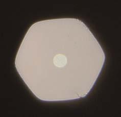
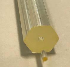
Figure 1: Highly Tm-doped Germanate double cladding fibre
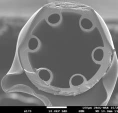
Figure 2: 10.6 μm guiding chalcogenide hollow-core fibre (left) and mode field diameter of the transmitted beam (right)
We will continue to focus on the improvement of both hollow-core and active fibres. For the hollow-core fibres, we aim to improve the drawn structures to achieve losses smaller than 1 dB/m from 4.5 μm to 12 μm. In addition, we will attempt the fabrication of a new class of hybrid AR-HCF that could potentially result in losses in the 1 dB/km in the same wavelength range (4.5 μm - 12 μm). Regarding the active fibres, we intend to demonstrate the advantage of the double clad Germanate fibres in practical ultra-short pulse amplification scenarios.
