
Annual Report 2021
■ Lead research in core photonics platform technologies: silica optical fibres, III-V semiconductors, silicon photonics, 2D materials and metamaterials.
■ Develop integrated manufacturing processes, making it simple and efficient to incorporate photonics into high-value systems.
■ Fund early stage research into cutting-edge manufacturing technologies.
expertise
state-of-the art
to:
The Future Photonics Hub is a partnership between two leading UK research institutes, the Optoelectronics Research Centre at the University of Southampton and the EPSRC National Epitaxy Facility at the University of Sheffield. We work with a network of over 40 companies, representing strategic UK sectors including telecommunications, healthcare, defence and aerospace, to support the rapid commercialisation of innovative photonics manufacturing technologies. Together, we are combining our
and
experimental facilities
Introducing the Future Photonics Hub 3 4 Contents Introducing the Future Photonics Hub 03 Our mission 04 Executive summary 06 Case studies 08 Bringing the Hub to life during and after COVID-19 10 The ultimate enabling technology 16 Core technology platforms 18 Innovation Fund 20 Research income 22 National leadership 24 Bringing photonics research to more diverse audiences 34 In the media 38 Technical reports 40 The team 64
|
We aim to secure the UK’s position as a leading innovator in the high value global photonics market by transferring new, practical and commercial process technologies to industry.
We bridge the gap between academic research and product development, uniting the UK science base with industry and funding agencies to co-invest in R&D.
We respond to the needs of industry by creating new photonics materials, devices and components, designed to be easy to manufacture and integrate with existing technologies.
We use innovation in light technologies to accelerate growth in the UK’s £14.5 billion photonics industry* and support UK manufacturing output across key global market sectors.
*Source: The Photonics Leadership Group (PLG), July 2021.
| Our
mission
5 4
In the six years since inception we have more than tripled the impact of our initial Government investment. We have generated more than £18 million of income from industry and are working on 81 research projects to help bring new photonics technologies to market. We have also been awarded an additional £16 million in competitively won grant funding to further accelerate next generation manufacturing research.
Launched virtual tours of facilities in Southampton and Sheffield to drive new business and partnerships during the COVID-19 pandemic.
Constructed a unique deposition apparatus with local SME, Themic Edge Ltd, to advance new ways of manufacturing emerging 2D materials on a large scale.
Taken an active role in the national technology agenda and moderated vibrant panel on ‘The decade of digital inclusion’.
Demonstrated the world’s most advanced integrated LIDAR system with US start-up company Pointcloud Inc.
Discovered that a deep learning neural network can predict the outcome of Focused Ion Beam milling process with high accuracy.
Returned to face-to-face events, bringing industry, academia and civil servants together to discuss ‘the UK photonics innovation chain,’ at Photonex in Glasgow.
Broken more world records in hollow-core fibre research.
Partnered with Southampton City Council to provide optics workshops to pupils who were Afghan refugees.
“ It’s been astounding to see game-changing innovations continuing to emerge from the Hub. We know that when scientists and engineers come together to think about manufacturing, they come up with new ideas. But it’s all about delivery and this year, we’ve seen one of our spinout companies, Lumenisity, go from strength to strength, building a fibre fabrication facility in the local area. A long term partnership in silicon photonics with Rockley Photonics has seen the company successfully break into the healthcare market and our work in high power lasers with a UK partner leads the charge towards next generation, low emission manufacturing. So much has been delivered and the exciting thing is, we’re just getting started.”
Together we are maximising the impact of Government investment and continue to make great strides in uniting the UK photonics community.
| Executive summary
Professor Sir David Payne Principal Investigator, The Future Photonics Hub
In 2021 we have
7 6
Optical Fibres - Lumenisity
Lumenisity was spun out from Southampton in 2016 and aims to commercialise discoveries in hollow core optical fibres which have demonstrated world-record data transmission with low losses. With increasing global volumes of data and requirements for faster speeds, hollow core fibre (HCF) provides a basis for next generation communications.
A project with BT and Open Radio Access Network (O-RAN) mobile vendor Mavenir at BTs R&D facility in Adastral Park is demonstrating the potential of the technology. The trial involves a 10km long HFC cable provided by Lumenisity (CoreSmart® hollowcore).
jobs are estimated to double to 160 by the end of 2023. Whilst some applications are commercially ready now, scaling up the manufacturing is the major challenge with Lumenisity estimating a further £100m of investment over 5 years being required.
Silicon Photonics – Rockley Photonics
Rockley is a UK start-up company developing process technologies for silicon photonics with a wide range of applications such as communications, guidance systems & medical devices.
Lumenisity is the global leader in HCF cables for telecommunications. It is the only fibre supplier capable of producing and cabling HCFs of low enough loss for telecommunications over more than 10km. The UK is globally leading by orders of magnitude ahead of the USA, Japan and China, due to EPSRC’s long-term involvement through Southampton.
Lumenisity is committed to UK manufacturing and is building its £20m production facility within 3 miles of Southampton University to allow its close relationship to continue. HCF will never replace solid fibre but will exist as a high performance niche within the market.
According to BT, such cables have the ‘potential to reduce the latency, or signal delay, caused by the light travelling through glass, by up to 50%.
‘This technology has the potential to make New York digitally closer to the UK than Europe. We want to see the first transatlantic HCF cable within 5 years. The collaboration with Southampton is the best I have seen by far. That is why we are building our factory within 3 miles of the University’. David Parker, Chairman, Lumenisity
The market for fibre optic cables was worth $10bn in 2021, with expected CAGR of 20% to reach $26bn by 2026 . Lumenisity forecasts that the global HCF cable market will potentially grow to 20% market share suggesting a market value of $5.2bn in 2026. Assuming Lumenisity retains its leading position, it is not unreasonable to suggest that it could have 20% of the HCF market with estimated revenues of $1bn from the UK in 5 years time.

Lumenisity has received significant investment and has created 80 high-skilled manufacturing and research engineering jobs. These
In addition, HCF investment will support growth in the UK economy including the UK’s financial services sector (£164.8bn in 2020), the gaming sector (£2.9bn in 2021) and the communications devices market (£3bn in 2021).
Rockley’s multi-micron waveguide platform was developed with assistance from the Hub to overcome fundamental challenges for high volume manufacturing of highly integrated optical/ electronic devices. Advantages include higher density waveguide circuits, better manufacturing tolerances, superior optical power handling, and a more efficient interface to the photonics IC. Together these elements enable improved performance and efficiency, while at the same time, reducing size, power usage, and cost.
A recent and significant development is a powerful spectrometer on a chip with

enhanced performance to measure chemical biomarkers. This has opened up the potential for wearable devices to measure human health indicators in real time. Immediate applications include diabetes monitoring and early diagnosis of cancer through measurement of metabolic changes.
Rockley estimates a total addressable market of $48bn with commercialisation to start in 2022-23. As at December 2021, 17 customers are contracted with discussions started with a further 54 and 100 plus identified as targets. Achieving even 1% market share will value its sales at $480m against a 2020 turnover of $22m and a $76m R&D spend. Manufacturing is likely to take place in the USA but Rockley will continue to employ development staff in the UK. This could not have happened without EPSRC funding.
High Power Fibre Lasers – SPI Lasers
SPI Lasers was spun out of Southampton in 1996, listed on the London Stock Exchange in 2005 and taken over by TRUMPF Lasers UK Ltd in 2008 in a $50m deal. It specialises in smart high-power fibre lasers (HPFL) in advanced manufacturing. These smart lasers allow processes such as welding, cutting, marking and micro-machining to be carried out faster and more accurately with better reliability, less waste and higher productivity. Advances in these lasers are based on two decades of research at Southampton which has continued through the Future Photonics Hub.
TRUMPF has customers in 130 countries with applications in automotive, medical, consumer electronics, materials processing and manufacturing. The market for HPFL has grown rapidly, with forecast global sales pre-COVID of £8.9bn by 2028, though the most recent estimate suggests $4.7bn by 2028.
Impact relating to HPFL based on EPSRC funded research are:
■ 303 direct jobs within SPI Lasers
■ £5-£10m annual cost saving due to reduced pump power requirements
■ New products worth an estimated £144m.
| Case
There is no doubt that the Hub has played a significant role in growing the photonics sector in the UK. Here we highlight some examples of impact.
studies
9 8
As the world adjusted to living with COVID-19, the Future Photonics Hub focused on bringing its virtualisation project to life to enable industry and the public to continue to engage with our world-leading researchers and facilities.
Continued restrictions and recurring lockdowns meant access to our labs, facilities, technologies and researchers remained difficult, so launching our virtualisation project as soon as possible became even more crucial if we were to continue to drive our work forward.
portal that went far beyond a simple website, providing an enhanced experience for the virtual visitor to mimic or exceed normal business interactions.
In 2020, we received EPSRC funding for an ambitious project to virtualise interactions with the outside world and create a unified
The aim was to produce highquality films showcasing our research and facilities, virtual laboratory visits, online events and meetings, video teaching resources and virtual workshops for teachers and children.
A year later and the team has gone above and beyond the call of duty to launch the majority of these materials, with the rest well underway. The team has included researchers, technicians, lab managers, cleanroom staff, estates and facilities and students.

“The whole team was incredible in helping us get camera crews into the labs to film the facilities,” said Hub Research and Relationship PR Officer Michelle Mitchell.
“There are already stringent protocols in place to gain access into these areas, many of which are carrying out sensitive research. On top of this, we had to ensure that we were working within COVID-19 safety
guidelines which meant adhering to lots of additional measures. The team were outstanding and worked really closely with us to enable us to film demonstrations, equipment and interviews.”
a window into spaces they physically can’t access at the moment. We have been able to bring to life the expertise of our community, as well as the incredible facilities.”
“These assets will allow us to continue vital conversations with new industrial partners. They provide companies and academics, who want to explore working with the Hub,
| Bringing the Hub to life during and after COVID-19
11 10
| Bringing the Hub to life during and after COVID-19
Virtual Tours
In March, we launched the first of our virtual tours which featured Southampton’s 20,000sq ft Cleanrooms The tour has already had more than 1,400 unique visits.
In September, our second virtual tour was launched of Sheffield’s National Epitaxy Facility


We continue to bring more facilities online and have shot our telecommunications, laser, silicon photonics, integrated photonics and quantum photonics labs. These will be launched in the coming weeks.
Showcase Films
We have launched six films showcasing the world-leading research and development being carried out at the Hub. These feature academics talking about our research expertise, facilities and laboratory space. They ask the question, What if? Exploring the potential light has to solve societal problems in innovative ways. What if light could save a life? What if light could help us understand each other better? What if laser technology could revolutionise manufacturing? They share our capabilities, our processes, the emerging technologies and their potential applications and have already been viewed 1,200 times. The films have been launched on YouTube, highlighted on our website and are being featured in University of Southampton alumni publications and research and innovation services newsletters. The films have been promoted on social media channels and in other digital newsletters and have been picked up by EPSRC news channels.
They will be embedded in the Virtual Tours to provide another layer of information and engagement.
The Future Photonics Hub –Redefining what’s possible

Introduces the Hub’s incredible facilities and expertise to de-risk ideas and show how new technologies can be made reproducibly, reliably and cheaply. Photonics can transform the existing capabilities of electronicsbased materials and devices, creating better or brand-new technologies. The Hub focuses on the manufacturing of these technologies.

Fibre Laser innovation – the future of green manufacturing


Discover how fibre lasers are having a profound impact on manufacturing and how the Hub is developing innovative technologies to be used in digital manufacturing. The unique properties of these novel lasers are resulting in a 30 per cent increase in speed, using half the power.
Optical Fibre innovation
Explores how the Hub is working with industry to drive innovations in optical fibre design and fabrication in one of Europe’s best academic cleanroom facilities. Our experts share our mission to secure the UK’s position as a leading innovator in the high value global photonics market by transferring new, practical and commercial process technologies to industry.
13 12
|
Bringing the Hub to life during and after COVID-19
Nanofabricating silicon photonics - electronics of the 21st century
Reveals how our silicon photonics chips with tiny wave guides have a cross-section of ‘a thousand times less than that of a human hair’. Our cleanroom tools and experts in fabrication techniques allow us to develop these chips that are being used in data centres, autonomous vehicles, point-of-care diagnostics and environmental sensing.
Integrated photonics - creating new materials, one atom at a time
Showcases how we are taking optical devices like lasers, LEDs or solar cells and intimately integrating them with electronics to create more complex devices, by mixing materials and making different types of semiconductor materials called compound semiconductors.
Novel glass innovation
The Future
Although these resources were initially designed and created to ensure business continuity during the pandemic, they are without doubt a high-value asset that will be used long into the future.
Michelle said: “They are an incredible resource, benefitting not only the Hub but also industry and external researchers, by opening a door on to the game-changing work that is carried out in our facilities. These resources have allowed people to access our academics and resources during a global pandemic but moving forward it will open up closed doors to potential collaborators or customers nationally and internationally who wouldn’t otherwise be able to make the journey to see our resources in person.
“What we do at the Hub is incredible but is not always easily understood by those outside who may not be able to see how it could help them unlock a problem or realise that photonics could provide the solution to take their business to the next level.”
Discover how we are redefining what’s possible in novel glass by asking new questions and finding new solutions. We share how we are working with industry to explore the fabrication of novel glass that can be used in a range of applications. 15 14
| The ultimate enabling technology
Photonics is the science and technology of light. Although most people do not realise it, photonics technologies are widely integrated into products and systems across a broad range of sectors.
Here are just a few examples of the many applications of photonics technologies.
Enabling key industry sectors
Harsh environment sensors for oil & gas
Laser-written diagnostics for healthcare
Optical fibres for high bandwidth telecommunications
Value £14.5bn industry value to the UK economy
Employment 76,700 people employed across the sector
Output £6.5bn total GVA £85,000 GVA per employee (vs UK manufacturing average of £67,000)
Growth 12% like for like growth over two years (5.8% CAGR)
Silicon photonics for data centres
UK photonics manufacturing industry
Putting the UK at the forefront of future industries
The UK is an international leader in photonics research. Our science base has already given rise to a globally significant market, which continues to expand at an impressive rate.
Photonics technologies are both ubiquitous and transformative. The UK photonics manufacturing industry is growing, as are many other high-tech industry sectors enabled by photonics. Investing in future photonics innovation is critical to retaining the UK’s competitive edge in the £400 billion global photonics market and offers vast potential to stimulate wider economic growth.
Head-up displays for aviation
Integrated photonics for quantum technology
Photonics has near limitless uses and can be found in almost all of the products and services we use in everyday life.
Sensors for security
LIDAR for autonomous vehicles
High power fibre lasers for green manufacturing
Source: The Photonics Leadership Group (PLG), July 2021
17 16
| Core technology platforms
Core Technology Platforms
1. Large-Scale Manufacturing of Metamaterials and 2D Materials
Developing cost-effective, reliable and volume-scalable methods to fabricate these novel materials in order to enable their practical exploitation in applications such as telecommunications, displays and sensors.
2. Light Generation and Delivery
User-driven manufacturing processes will increase the integration and unification of diverse manufacturing platforms in III-V epitaxy, metamaterials, Si-SOI fabrication methods and functional fibre geometries.
Grand Challenge: Integration
We aim to develop the important ‘Pervasive Technologies’ identified in the UK Foresight report on the future of manufacturing through carrying out research into four, carefully selected Technology Platforms: High Performance Silica Optical Fibres, Light Generation and Delivery, Silicon Photonics and the Large-Scale Manufacturing of Metamaterials and 2D Materials.
Our consultations with over 40 companies, Catapults and Innovative Manufacturing Centres identified a clear business need to reduce the complexity of incorporating next generation photonics technologies in high value systems.
Integration is an industry wide issue which we have chosen to tackle as our ‘Grand Challenge’.
■ Our innovations navigate airliners, cut steel, mark iPads, manufacture life-saving medical devices and power the internet.
■ Our optical fibres, invented and made in Southampton, are on the Moon, Mars and the International Space Station.
■ Our epitaxial wafers and devices, produced in Sheffield, have enabled world-class semiconductor research in the UK since 1979.
We also know that the key to producing low cost components and systems is integration. Optical fibres, planar waveguides, metamaterials and III-V semiconductors cannot yet be combined in a cost effective, integrated manufacturing process.
Our research capabilities
The Hub is a unique partnership between the Optoelectronics Research Centre (ORC) at the University of Southampton and the EPSRC National Epitaxy Facility at the University of Sheffield. It is this collaboration between two leading research institutes that ensures our work is characterised by scientific excellence and innovation. Together, we have an extensive and impressive track record in research and enterprise:
■ Our combined portfolio of startups now exceeds 12 companies.
■ Our expertise is underpinned by our £200 million of state-of-the-art fabrication facilities.
The drive to achieve integration is a ubiquitous theme uniting the world’s photonics industries. The photonics industry today can be likened to the early days of electronics when individual components were wired together, resulting in inevitable cost and scaling implications. Today’s photonics components are not yet compatible with a single manufacturing platform and this represents a major industrial challenge.
3. High Performance Silica Optical Fibres
Optical fibres are essential components in many photonic devices and systems – from sensing to amplifying light. The key challenge in manufacturing fibre is improving its loss, gain and power handling characteristics.
4. Silicon Photonics
Achieving integration with optical fibres, light sources and key processes of wafer level manufacturing to enable devices such as low cost transceivers for data centres and mid-infrared sensors.
We are developing new photonics technologies to fuel innovation. Our research is delivering solutions to manufacturing challenges and overcoming barriers to the widespread industry adoption of next-generation photonics.
19 18
Since 2016, we have awarded just over £780,000 in grant funding to projects led by UK researchers offering new capabilities relevant to industry but outside of our core expertise.
Over the years we have awarded projects to researchers in institutions including the universities of Oxford, Cambridge, Bristol, Bangor, Southampton and Strathclyde.
In partnership
Our most recent call was launched in May 2021 in partnership with other EPSRC Future Manufacturing Research Hubs to jointly fund projects that exploit research synergies and allow access to a wider range of facilities and equipment.
Partnering with the EPSRC Future Manufacturing Research Hubs in Composites, Electrical Machines and Metrology, we offered up to £900,000 in funding to support a number of feasibility studies. £200,000 was awarded to
the following four photonics projects:
Novel, Embedded and Robust Optoelectronics to Value Engineer Precast Concrete Dr Brian Sheil, University of Oxford
Practical sustainability goals can be achieved by minimising concrete consumption and extending the life of built infrastructure. This project will explore the feasibility of developing and embedding novel ultra-low-cost optoelectronic sensing systems in precast construction elements for buried utility infrastructure.
Disruptive Photonics Manufacturing for Ocean’s Dissolved Methane Monitoring
Dr Rand Ismaeel, University of Southampton
This project will further develop a novel writing technology to make the next generation of photonics marine sensors compatible with miniaturised autonomous underwater vehicles. They will create a cost-effective monitoring tool that can revolutionise how the oil and gas industry perform leak detection.
Pyroelectric PZT Thin Films Integrated on Si for Efficient IR Detectors
Dr Ioanna Bakaimi, University of Southampton
Integrated detectors are needed to realise the full potential of silicon photonics in mid-IR sensing. This project aims to enable integration of efficient room temperature pyroelectric IR detectors on the silicon photonic platform using lowcost materials and a direct, reliable growth technique.
Wafer-scale Manufacturing of Large Area Metasurfaces Using a Deep-UV Scanner
Professor Otto Muskens, University of Southampton
This project aims to enable deep-UV wafer scanner and track tools to produce near- and mid-IR metasurfaces with applications in IR imaging and sensing. They aim to address the gap between small-area demonstrators using e-beam lithography and FIB, and the need for large area, scalable manufacturing methods.
The Future Photonics Hub
University of Southampton University of Sheffield
Innovation Fund partners
Heriot-Watt University University of Bangor University of Bristol University of Cambridge University of Oxford University of Southampton with Imperial College, London University of Southampton with Phoenix Photonics University of Strathclyde Industry partners
International industry partners by country UK photonics industry activity
Sweden
China Japan South Korea Italy
Canada Germany Saudi Arabia 21 20
| Innovation fund
With support from our £1 million Photonics Innovation Fund, we are building a national network of academic partners, primed to respond to emerging industrial challenges with a wide range of expertise.
USA
Innovating with industry for economic growth.
As national leaders in photonics manufacturing research, we stimulate collaborations between academia and industry throughout the supply chain.
We engage industrial influencers to raise awareness of the value of photonics, both in delivering transformational manufacturing technologies and driving economic growth.
We have secured significant income in all four Technology Platforms, working with companies across the photonics supply chain from component manufacturers to large end-users in a range of market sectors. Our ramped-up activities under the Grand Challenge of Integration have also been supplemented by some targeted projects following the award of funding from the Defence and Security Accelerator (DASA).
| Research income
£6,113,000 £3,755,000 £2m+ 2021 industrial income £18m+ Total industrial income £16m 36% competitively secured income 81 projects, 4 Technology Platforms 2016-2021 9 industry sectors 2016-2021: sensing, defence, photonics, data comms, storage, LIDAR for autonomous vehicles, aerospace, advanced materials and manufacturing Industrial income by Technology Platform 2016-2021 2016-2021 2016-2021 2016-2021 Total income £6,403,000 £10m 23% core income Total income January 2016 to December 2021 High-Performance Silica Optical Fibres Light Generation and Delivery Silicon Photonics Large-Scale Manufacturing of Metamaterials & 2D Materials Integration £1,411,000 £18m 41% Industry income £657,000 23 22
Our role is to increase awareness and engagement with the ways photonics manufacturing research is tackling Grand Challenges, improving people’s lives and boosting productivity. We provide access
the world, giving keynotes and plenary talks, presenting papers and exhibiting technology demonstrators.
to expertise which helps industry innovate and champion strategic investment that will drive social and economic impact.
Although COVID-19 disrupted the usual in-person events, we have still been able to continue delivering our research to some of the largest and best-known international conferences and exhibitions.
The sessions were chaired by John Lincoln, CEO of the UK Photonics Leadership Group, and panel members considered support for translational photonics research in the UK, bringing difference perspectives on what is needed to convert world-class research and development into products in the global marketplace.
Conferences and exhibitions
Playing an active leadership role on the conference and trade show circuit is one of the most powerful ways to engage stakeholders and represent the community on a global stage.
Since 2016, we have participated in more than 100 conferences, trade shows and workshops around

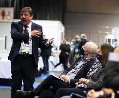
SPIE Photonex 2021 in September was the first in-person post COVID-19 exhibition and conference and the Hub was excited to be playing a part in the exhibition, the industry programme and the conference.
We supported two panel discussions, inviting key members of the UK’s innovation ecosystem and industry representatives to tackle the question of ‘The UK Photonics Innovation Chain: What Can We Do Better?
The discussions were set in the context of the current UK photonics landscape and developments in wider innovation policy and were stimulating and robust, sparking dialogue and constructive debate about what works well, where there is room to do better, and gaps in the innovation chain. Read the full story here.
As the national photonics manufacturing hub, we are responsible for providing leadership to the UK academic, industrial and government communities.
Industry panel debating the UK photonics supply chain
Returning to our first in person event at SPIE Photonex in Glasgow
| National leadership 25 24
Local MP actively participating in the panel discussion - ask JL for his name.
Future Photonics
photonics technologies.
During the last year, we have published a series of features showcasing initiatives where the Hub is both influencing and reacting to the national photonics landscape.
Championing photonics and its role in reaching net zero
Carol Monaghan MP – a champion for the photonics sector in Westminister – actively engaged with the Future Photonics Hub discussion panel for photonics leaders from industry and academia at Photonex 2021. We spoke to her about her special interest in photonics and she shared her thoughts on:


■ The critical role photonics will play in reaching net zero
■ Society’s biggest challenges in achieving climate goals and how photonics will help
■ What environmental issues photonics will help to tackle
■ What role a national manufacturing hub like the Future Photonics Hub plays in making greener technologies a reality
■ How the government could help achieve these aims
Carol is MP for Glasgow North West and has a degree in laser physics and optoelectronics and a 20-year career as a physics teacher. She established the AllParty Parliamentary Group on Photonics and Quantum and is keen to see the realisation of the huge environmental and economic potential of optical technologies.
Read the full story here.
A key role of the
Hub is to demonstrate national leadership in manufacturing the next generation of
| National leadership
27 26
Bringing quantum research into manufacturing of the future
The National Epitaxy Facility at the University of Sheffield, one of the Future Photonics Hub’s two partner institutes, is pioneering the development and commercialisation of world-leading quantum science and technology based on semiconductor quantum dots.
Quantum dots are comprised of nanometer-sized materials that behave in a similar fashion to isolated atoms have already been commercialised and used in lasers and LEDs, with the most common
Advancing infrastructure and boosting productivity using fibre vibration monitoring and detection
More than a decade ago, Southampton Senior Research Fellow Dr Ali Masoudi devised a distributed acoustic sensor (DAS) that can measure vibration in realtime along a fibre optic cable.
He is now working with international organisations to improve the way railways are monitored and how subsea cables can be protected.
The Hub has supported his research by using its expertise to test the system and helping to establish relationships and collaborations with industry. Ali has been able to use feedback from these companies to improve the sensors and meets the company’s needs.
Read the full story here.
application being QLED TVs.
They are a particularly important source of single photons of light, which can be used in many important quantum science experiments but are also of great commercial significance as the building blocks for quantum computers and ultra-secure quantum communication systems.
Professor Jon Heffernan, Deputy Director of the Future Photonics Hub and lead of the National Epitaxy Facility, outlined how the Hub is exploring more advanced quantum dot technology looking at the use of the more esoteric quantum properties of the dots.
Read the full story here.
New Chair of the Hub Advisory Board shares her thoughts on the role of the Hub
New Chair of the Hub Advisory Board Dame Frances Saunders has held some of the most influential positions in physics and engineering including Chief Executive of Dstl, President of the Institute of Physics and Trustee at the Royal Academy of Engineering.
Dame Saunders became British Leyland’s first female graduate engineer in 1975 and has spent her career promoting science, engineering and leadership, especially to young people.
We talk to her about the role of the Hub, it’s ambition and what it has been like working in a male dominated industry.
Read the full story here.
Unlocking new data on ocean greenhouse gas emissions


Researchers at Southampton’s Optoelectronics Research Centre, one of the Future Photonics Hub’s two partner institutes, and the National Oceanography Centre Southampton are developing a new generation of smart, low-cost optical sensors capable of detecting greenhouse gases and pollutants in our oceans.
The technology is set to revolutionise ocean monitoring
techniques and will enable scientists to answer urgent questions about global warming processes for the first time.
Combining the power of photonics and nanotechnology, the team is incorporating highly sensitive optical fibre isotope detectors into miniature autonomous underwater vehicles.
Read the full story here.
| National leadership
29 28
How fibre lasers can help save the planet
High power fibre laser technology boasts many unique features that set it apart from other competing technologies and could be the key to making manufacturing more efficient and sustainable.
High power fibre lasers are now routinely produced around the world and widely used in the most advanced production lines for cutting, welding and 3D printing.
Professor Michalis Zervas, a Hub Co-Investigator, shares his expertise on the environmental benefits of fibre laser technology and its potential as the industry enters the digital manufacturing era.

Read the full story here.

Investing in the next generation of photonics leaders

Early Career Researcher, Dr Natalie Wheeler knows the challenges she and her peers face when trying to ‘cross the barrier’ from postdoc to research group leader.
Space to develop ideas while having the support of colleagues and line managers who see the bigger picture, along with a funding source that
provides longevity, are all needed to become an independent researcher.
Natalie reveals how she has experienced this on her way to being appointed as CoInvestigator at the Hub.
Discover more about Natalie’s journey here.
A roadmap to meet the demand for silicon photonics fabrication in the UK
Silicon photonics technology uses silicon as a platform for photonic circuits to create the next generation of highly integrated optical communication systems and data infrastructure.
The silicon photonics market exceeded $600m in 2019 and is poised to grow at 30 per cent CAGR between 2020 and 2026, with the need of silicon photonics in data centre application areas continuing to drive the market forward.
Callum Littlejohns is Coordinator of the CORNERSTONE programme, a silicon photonics rapid prototyping fabrication service based at the University of Southampton. He shares his insights into the current UK silicon photonics research space and the direction it may take over the next decade, looking at how CORNERSTONE is helping to meet the current demand, what new platforms they are working on and how the Hub can support the work.
Read the full story here.
Rebuilding the UK telecommunications industry
The UK’s telecommunications industry contributes four to five per cent of the country’s GDP and plays a vital role in its economic and social well-being.

In the late 1990s/early 2000s, the UK had a very healthy telecommunications industry doing world-leading research and was home to large UK-owned manufacturing companies. However, today there are few major UK-owned telecoms companies and we have a relatively modest telecoms-centric manufacturing capability.
Professor David Richardson, Hub Co-Investigator and Deputy Director of the Optoelectronics Research Centre, has been at the forefront of photonics research for the past 30 years.
He shares his insights on the current state of the UK’s telecommunications networks and what needs to be done to ensure they keep up with society’s demand. He outlines the activities that are being carried out to address this challenge.
Read the full story here.
| National
leadership
31 30
Keynotes and plenaries
In March of 2021, Future Photonics Hub Co-Investigator
Professor Graham Reed delivered a Plenary at Photonics West Digital Forum, centred on the dramatic work in silicon photonics being spearheaded in the University of Southampton.
Photonics West is the world’s premier lasers, biomedical optics, and optoelectronics event, providing a platform for world-class speakers to share the industry’s latest challenges and advances.
In September of 2021, the Future Photonics Hub returned to it’s first in person event with conviction at the SPIE Photonex and Vacuum Expo. Taking an exhibition stand and sponsoring two panel discussions about the UK’s innovation ecosystem.

Graham described the technology as game-changing for data communications, as well as applicable to an increasing number of other applications.


In September of 2021, Professor Sir David Payne moderated vibrant debate at a Marconi Society panel on, ‘The decade of digital inclusion: Issues that keep us up at night.’

Experts from technology, policy, and digital inclusion will join forces to describe what the future could look like, the questions we need to answer, and the different points of view we have to consider.
https://twitter.com/ISOC_Live/ status/1438005895913431042
Accolades
Hub Principal Investigator, Professor Sir David Payne became the eighth recipient of the Berthold Leibinger Zukunftspreis awarded by the German foundation Berthold Leibinger Stiftung.
A jury of renowned international experts and industry leaders recognised Professor Payne’s work on the erbium-doped fibre amplifier (EDFA), high power fibre lasers, and his pioneering research in fibre optics technology.
National leadership 33 32
|
| Bringing photonics research to more diverse audiences
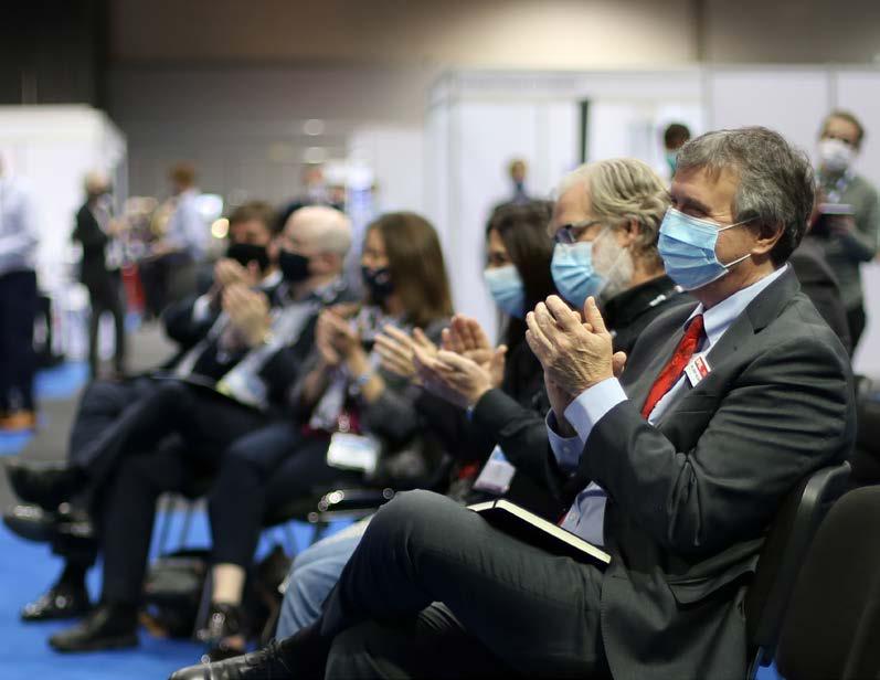
As more people were vaccinated towards the end of the year we were able to restart face-to-face events.
Our work during the year focused on:
■ demonstrator training and the delivery of on-line workshops with the science-interested public at science festivals;

■ support for a summer school for A-Level physics students of AfroCaribbean Heritage;
■ face-to-face workshops with a small group of Afghan refugees;
■ work on the virtualisation of Hub activities;
■ disseminating good practice at national public engagement and outreach conferences.
Reaching the disadvantaged
We impacted almost 550 members of the public, many who were disadvantaged by a lack of access to technology. We contributed optics activities to outreach packs distributed to local community groups.
Student skills development
We provided two workshop sessions for seven postgraduate and two undergraduate physics students, followed by on-the-job training and on-going self-reflection activities. The sessions included an introduction to the Hub and the purpose of photonics outreach and public engagement.
The continuing COVID-19 global pandemic severely impacted the Hub’s Schools’ and Public Engagement Programme again during 2021, however, opportunities for working with new and often minority audiences in new ways emerged.
35 34
Image credit: Ollie Lane
| Bringing photonics research to more diverse audiences
Postgraduate student Callum Stirling said: “Outreach training improved my ability to communicate my research, with direct benefit to the quality of my research outputs such as journal papers and my doctoral thesis.
Engaging with community groups
Continuing virtualisation of Hub outreach and public engagement
“Engaging in outreach activities was crucial to my success delivering conference presentations and working with external collaborators. Planning and delivering outreach events developed skills in leadership, project management, stakeholder engagement and financial control. These skills have directly led to my success in finding employment in photonics following my doctoral studies.”
We partnered with Southampton City Council to provide an optics workshop to pupils who were Afghan refugees. The children had recently arrived in the UK and did not speak English. The workshop, which was translated into Farsi, focused on fibre optics and involved participants building their own kaleidoscopes.

Following the success of our first Light Express video ‘Exploring Waves of Light’, we started producing a second film featuring Southampton graduate Dr Senta Jentzen that focuses on measuring the speed of waves. The film is due to be published very soon.

Activity delivery
We delivered on-line optics workshops at the Southampton Science and Engineering Festival Family Day (SOTSEF) and the celebration of the International Day of Light, which gave families the opportunity to find out more about photonics and make spectroscopes from household objects. The workshops were designed to appeal to a wide age-range as well as family groups.
The Hub outreach team also supported a Southampton physics summer school for students of AfroCaribbean Heritage by contributing funding and providing a virtual tour of Hub facilities. Students from Afro-Caribbean heritage face significant barriers to studying physics, and work is being done to increase diversity in photonics. The summer school included physics and astronomy talks and practical activities and an introduction to the Hub by a postdoctoral researcher.
Dissemination of Best Practice
Southampton postgraduate student
Alice Iles gave a talk about our on-line activities at V-Interact - an engagement workshop for the physical sciences – to an audience of researchers and public engagement professionals.
We also delivered four face-to-face hands-on workshops during the Southampton Festival of Arts and Humanities.
Widening participation across he digital divide

During lockdown hundreds of pupils in Southampton had little or no access to the Internet, effectively excluding them from educational activity. We contributed activities for 350 activity packs that were distributed via Southampton’s Widening Participation team to local underserved schools.
Dr Pearl John, Public Engagement Leader, gave two presentations at workshops during the annual National Coordinating Centre for Public Engagement (NCCPE) ‘Engage’ conference. The presentations focused on improving outreach and public engagement experiences for autistic people at photonics outreach events. The workshops were attended by 40 outreach and public engagement specialists and interested others.
 Image courtesy of: Ollie Lane
Image courtesy of: Paul Gow
Image courtesy of: Dr Pearl John
Image courtesy of: Ollie Lane
Image courtesy of: Paul Gow
Image courtesy of: Dr Pearl John
37 36
Image courtesy of: Dr Pearl John
Ofcom has identified ground-breaking advances in fibre optics and silicon photonics technologies that will shape communications of the future.
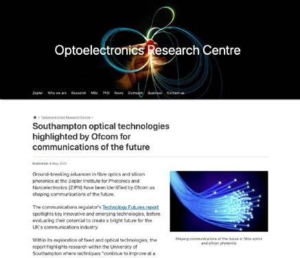
The communications regulator’s Technology Futures report spotlights key innovative and emerging technologies, before evaluating their potential to create a bright future for the UK’s communications industry.
The Ofcom report which was co-authored by Optoelectronics Research Centre Visiting Professor William Stewart, explores the merits of hollow-core fibre technology in surpassing current fibre limits.
To mark International Women in Engineering Day on 24 June 2021, Early Career Researcher Dr Natalie Wheeler spoke to BBC Radio Solent about her research into the next generation of optical fibres.
We announced the creation and use of a new type of hollow-core optical fibre to make a light-based gyroscope 500 times more stable than previous devices.
The story was picked up by external press outlets such as Physics World and the Royal Academy of Engineering.
Technical outlets such as TechXplore and Laser Focus World picked up on the narrative about how fibre lasers are having a profound impact on manufacturing, sharing news that the Future Photonics Hub is developing new technologies that will be used in the digital manufacturing era.
Several world record-breaking results in hollow-core fibre research received regular traction with the technical media with news coverage in titles such as Laser Focus World and Optics.org.
| In the media
39 38
Technology reports Long-Term Optical Performance of Hollow-Core Fibres 42 Short-wavelength operation (<1950 nm) of Cladding-pumped Thulium Fibre Laser in a Power Scaleable Fibre Design 44 Advanced Beam Shaping in High Power Fibre Lasers 46 Integrated Silicon Photonic Circuits 48 AI-Assisted Nanofabrication 50 Manufacturing 2D Materials 52 Directional VCSELs and Diffractive Optics for 3D Machine Vision 54 Development of Integrated Mid-Infrared Photonic Devices and Systems 58 Novel Forms of Interconnection and Device Integration for Emerging Multimode, Multicore, Hollow-Core and Multi-Component Optical Fibres 60 Progress on Wideband Optical Amplifiers 62 Images in University of Southampton’s £200m cleanroom complex 41 40
Long-term Optical Performance of Hollow-Core Fibres
Challenge
To assess the long-term optical and mechanical performance of hollow-core fibres (HCFs) in environments and configurations relevant to future deployment in various applications. To develop techniques and fabrication processes to mitigate any reliability or aging effects observed.
Progress
HCFs are a specialty optical fibre where light is guided in an air core, surrounded by a carefully designed cladding structure, consisting of thin glass (usually silica) membranes (see Figure 1a). In recent years, advanced fibre design and improved fabrication methods have significantly reduced the minimum loss achievable in a HCF [1] and these fibres are now being deployed in various applications, including telecommunications [2]. Beyond low loss, HCFs are particularly attractive for telecommunications as light transmission in an air-filled core significantly reduces non-linearity and latency (transmission time) as compared to conventional fibres where light is transmitted in glass. However, the long-term performance of these fibres is as yet largely unexplored and is a critical factor for future success. The impact of the gas composition and pressure inside the holes which run along the length of these novel fibres could be important in this long-term performance.
This year, we have focused on investigating the impact of the gas inside the core on the consistency of a HCF’s optical properties. We have previously shown that the gas pressure inside the holes of a HCF immediately post-fabrication is much lower than atmospheric [3]. Now, we have been studying the consistency of the transmission properties of different HCF designs when the fibres are exposed to atmospheric air over long time periods.
Here we show initial results from a nested antiresonant nodeless fibre (155m, NANF, Figure 1a); this type of HCF which was chosen as this fibre design is very similar to that recently used to demonstrate record low loss HCF transmission [1]. The fibre under test was sealed immediately after fabrication (to avoid atmospheric gas ingress until the experiment started). The fibre was then spliced at the optical input end to allsolid fibre (to provide a consistent coupling of light into the fibre) and the output end was opened up to atmospheric gas species and the fibre was kept in a laboratory (22, 40%RH (relative humidity)). The transmission of the fibre was then carefully recorded periodically over ~ 1 year.
Co-Investigator contact: Dr Natalie Wheeler nvw1v10@orc.soton.ac.uk

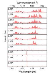
Figure 1: (a) A SEM image of a HCF (NANF design).
(b) The evolution of the transmission spectra through the NANF for different measurement days after opening the fibre end to atmospheric gas.
(c) The change in the loss of the NANF at 1550.2 nm.
(d) The evolution of the water vapour absorption within the NANF based on the water vapour absorption feature at 1441.4 nm.
The transmission spectra through the NANF recorded for different days after opening up to atmospheric gas are compared in Figure 1b and overall shows no significant changes (considering the measurement uncertainty) over the time period measured up until this point. This reliability of the NANF transmission is highlighted in Figure 1c which shows the fibre transmission over time at a wavelength of 1550.2 nm. Degradation of the optical performance was not observed even after 304 days of atmospheric exposure. During this measurement, the evolution of water vapour absorption within the NANF was also observed in the wavelength range between ~1300 and 1450 nm. As an example, the evolution of the water vapour absorption line at a wavelength of 1441.4 nm is shown in Figure 1d. The dramatic increase for the first ~8 days was due to the initial sub-atmospheric pressure of the post-fabrication HCF [3] and the following reduction was attributed to absorption of water vapour onto the silica surface within the fibre’s core [4]. The results shown here indicate that this water vapour absorption has negligible impact on the transmission of this type of HCF and this may be because of the very small fraction of power overlapping with the glass surface defining the hollow core, further work is ongoing to study this in more detail.
Future plans
The work described is part of a larger ongoing study into the performance of different HCF designs in a variety of different environmental conditions which are relevant to their deployment in a range of applications, including telecommunications.
References
[1] H. Sakr et al. “Hollow Core NANFs with Five Nested Tubes and Record Low Loss at 850, 1060, 1300 and 1625 nm,” in Proc. 2021 Optical Fiber Communications Conference (OFC) 2021, F3A.4 1-3.
[2] euNetworks Fiber UK Limited, “euNetworks deploys Lumenisity Limited CoreSmart hollow core fibre cable in London,” Apr. 14 2021. [Online]: https://eunetworks.com/app/uploads/2021/04/euNetworksdeploys-Lumenisity-Hollowcore-Fibre-in-London FINAL.pdf
[3] S. Rikimi et al. “Pressure in As-drawn Hollow Core Fibers,” in OSA Advanced Photonics Congress (AP) 2020, paper SoW1H.4
[4] S. Rikimi et al. “Comparison between the Optical Performance of Photonic Bandgap and Antiresonant Hollow Core Fibers after Long-Term Exposure to the Atmosphere,” accepted for presentation at OSA Optical Fiber Communication Conference (OFC) 2022.

| High Performance Silica Optical Fibres | High Performance Silica Optical Fibres
43 42
| High Performance Silica Optical Fibres | High Performance Silica Optical Fibres
Short-wavelength operation (<1950 nm) of Cladding-pumped Thulium Fibre Laser in a Power Scaleable Fibre Design


Co-Investigator contact: Professor Jayanta Sahu jks@orc.soton.ac.uk
Challenge
Two-micron lasers are of great interest for a range of applications in laser surgery, plastics processing, spectroscopy, and pumping of mid-IR sources. Tm-doped silica fibres (TDFs) are the preferred gain medium for power scaling of 2 μm sources as well as they are capable of operating in the wavelength range from < 1700 nm to 2100 nm. By optimising the glass composition within the TDF core, a two-for-one cross-relaxation process can be exploited, that enables Tm-doped fibre laser (TDFL) efficiency to reach well above its quantum limit with 79xnm pumping.
An efficient cross-relaxation process requires a high Tm concentration resulting in a high core numerical aperture (NA) that degrades the beam quality in a large core fibre. Furthermore, the strong three-level nature at the short wavelength side of Tm emission band poses significant challenges for 79xnm cladding-pumped TDFLs to operate below 1950 nm with high efficiency that can be achieved at long wavelengths.
Progress
Our research has focused on the development of TDF through engineering the core glass composition and tailoring the rare-earth doping profile that enables TDFL to operate at short wavelengths with a good output beam quality. Important fibre design features include a high Tm-concentration of >3 wt% to promote crossrelaxation process when cladding-pumped at 79xnm and a large core with a confined Tm-doping region to reduce signal reabsorption while maintaining an adequate pump absorption in a double-clad TDF.
Figure 1: (a) Refractive index profile of confined Tm-doped fibre and (b) Optical spectra of tunable TDFL.

Figure 1a Figure 1b
Figure 1 (a) shows the refractive-index profile of confined TDF. A 19 μm diameter core, with NA 0.19, has a central 6 μm confined Tm-doped region. The octagonal inner cladding has a diameter of 80 μm and is coated with a low-index polymer providing the cladding NA of 0.46. The small-signal pump absorption is 7 dB/m. The TDF with confined doping has been tested for tunable laser operation in a Littrow-configuration using a diffraction grating (300 lines/mm). We obtained a continuous tuning and stable operation of the laser from 1850 nm to 1980 mm, as shown in Figure 1b. Throughout the tuning range, the output power of the laser was marinated above 5W, which was primarily limited by the optics and launched pump power. We measured the beam quality factor (M2) as 1.2. The laser slope efficiency has reached >50% across this tuning range with a maximum efficiency of 60% at 1880nm has been obtained. We also achieved 21W of output power at 1880 nm and 15W at 1850 nm by placing the TDF in a water bath. Further optimisation of the laser design would offer the prospect of power scaling of TDFL in the short-wavelength side of the Tm transmission band with a good output beam quality using the confined-doped fibre design.
45 44
Advanced Beam Shaping in High Power Fibre Lasers
Challenge
Structured light, with spatially varying phase or polarization distributions, has given rise to many novel applications in fields ranging from optical communication to laser-based material processing. However, the efficient and flexible generation of such beams from a compact laser source at practical output powers still remains a great challenge. Here we describe an approach capable of addressing this need based on the coherent combination of multiple tailored Gaussian beams emitted from a multicore fibre (MCF) amplifier. We report a proof-of-concept structured light generation experiment, using a cladding-pumped 7-core MCF amplifier as an integrated parallel amplifier array and a spatial light modulator (SLM) to actively control the amplitude, polarisation and phase of the signal light input to each fibre core. We have demonstrated the successful generation of various structured light beams including high-order linearly polarized spatial fibre modes, cylindrical vector (CV) beams and helical phase front optical vortex (OV) beams.

Use of the MCF architecture provides for a highly integrated array of amplifiers and drastically reduces system complexity by enabling sharing of components across the multiple spatial channels, e.g. isolators, pump diodes and the SLM beam shaper that we used to control the amplitude, phase and polarization state of the signal light launched into each of the individual cores. Furthermore, since all the cores experience similar thermal and mechanical perturbations due to their very similar and close physical proximity, the environmental sensitivity of the relative phase and polarization between signals propagating through the different individual cores is substantially reduced compared to the case of arrays of physically separate single core fibre amplifiers. This leads to a corresponding reduction in active beam control requirements.
Scalar LP mode generation: We examined the generation of various higher order scalar linearly-polarised (LP) fibre modes by adjusting the input wavefront to the MCF amplifier. Here, we placed the relevant phase-plate of the desired LP mode in front of the LPO to construct the relevant correlation-filter. A few theoretical examples of the complex amplitudes for the individual beamlets required to generate specific LP modes are illustrated in Figure 2, along with theoretical and experimental far-field beam profiles. The experimentally measured far-field beam profiles agree very well with the corresponding theoretical predictions indicating that the complex amplitude of the individual beamlets is controlled as required.
Progress
In our research, we have demonstrated experimentally the generation of various forms of complex beam (including azimuthally phase-chirped OV beams and radially/ azimuthally polarized CV beams defined on the higher-order Poincaré sphere) by coherent combination of individually amplified signals in a MCF amplifier (see Figure 1).

Co-Investigator contact: Professor Michalis Zervas mnz@soton.ac.uk Figure 1
Figure 1: Schematic of the experimental setup. A single seed laser beam is adaptively shaped by a spatial light modulator (SLM) beam-shaper and the resultant field used to excite the individual cores of the MCF amplifier; multiple amplified beams are coherently combined to obtain various spatial modes in the far-field.

Figure 2: Scalar linearlypolarised (LP) mode generation. Idealised complex amplitudes of the individual cores required to generate specific LP fibre modes and the corresponding beam profiles in the far-field (in theory and measurement)
Figure 2
Future Plans
This work paves the way to the generation of high power and reconfigurable structured light beams from simple and compact laser sources. The switching and high power structured light beams may offer advantages in a wide range of applications such as laser material processing, free-space optical communication and high-resolution imaging.
High
47 46
|
Performance Silica Optical Fibres | High Performance Silica Optical Fibres
Integrated Silicon Photonic Circuits
Challenge
In the last 12 months we have focused on tackling two main research challenges: realisation of integrated near-IR circuits and systems (transceivers and LIDARs) and fabrication of wide band mid-IR photonic devices for spectrometers on chip.
Progress
We have developed a LIDAR with San Francisco start-up company, Pointcloud Inc. Fabrication is carried out at Southampton, using industry like processes, to trial and prototype devices and sub-systems. Following proof of principle, the company then incorporated the devices into systems that were fabricated in a commercial foundry. The work published in Nature (590, p256 (2021)), used a combination of foundry chips, a University of Southampton optical modulator, and company developed system software. The work demonstrated the most advanced integrated LIDAR system in the world to date, with accuracy of 3.1 mm at a range of 75 metres, using only 4 mW of light [1]. The system architecture is shown in Figure 1.
Two important devices needed for spectrometers on chip have been demonstrated: wide band MMI splitter and broadband single mode waveguides. Both are based on subwavelength gratings and both show low losses. The waveguides were single mode from 2 to 4 μm and exhibited a propagation loss of 1.55 dB/cm across this range.

Operational range of the MMI splitter (see Figure 2) was 3.1 - 3.7 μm thus exhibiting a two-fold bandwidth enhancement over a conventional MMI around 3.4 μm, when considering imbalance and insertion loss (600 nm vs 300 nm). Importantly, this highperformance bandwidth was achieved using devices that have a small footprint and can be fabricated simply, with a single lithography and etch step, on a 500 nm-thick SOI platform [2].
Co-Investigator contact: Professor Goran Mashanovich g.mashanovich@ soton.ac.uk

| Silicon Photonics Figure 1: LIDAR system architecture.
Figure 2: Wideband 2x2 MMI splitter.
Future plans
Future work will involve performance improvements of silicon near-IR and mid-IR devices and circuits, and will focus on: fabrication of more efficient optical modulators, integration of sources and room temperature mid-IR detectors, and realisation of spectrometers on chip.
References
[1] C. Rogers, A. Y. Piggott, D. J. Thomson, R. F. Wiser, I. E. Opris, S. A. Fortune, A. J. Compston, A. Gondarenko, F. Meng, X. Chen, G. T. Reed and R. Nicolaescu, “A universal 3D imaging sensor on a silicon photonics platform,” Nature, vol. 590, pp. 256–261, 2021, https://doi.org/10.1038/s41586-021-03259-y
[2] C. Stirling, R. Halir, A. Sánchez-Postigo, Z. Qu, J. Reynolds, J. Penadés, G. Senthil Murugan, A. OrtegaMoñux, J. Wangüemert-Pérez, Í. Molina-Fernández, G. Mashanovich, and M. Nedeljkovic, “Broadband 2x2 multimode interference coupler for mid-infrared wavelengths,” Opt. Lett. 46, 5300-5303 (2021). https://doi.org/10.1364/OL.439985
Silicon
|
Photonics
49 48
| Large-Scale Manufacturing of Metamaterials and 2D Materials
AI-Assisted Nanofabrication
Co-Investigator contact: Professor Kevin MacDonald kfm@orc.soton.ac.uk
Challenge
Focused ion beam (FIB) milling is a vitally important direct-write process for rapid prototyping and materials/device characterisation in both fundamental research and industrial manufacturing of nano-/microtechnologies. However, establishing process parameters for any specific task is a multi-dimensional optimisation challenge, typically undertaken by iterative (i.e. time-consuming and therefore costly) trial-anderror.
Progress
We have shown that deep learning – a neural network trained on the basis of prior manufacturing experience – can predict the outcome of FIB milling processes with high accuracy, taking account of instrumental and target-specific artefacts. Predictions are generated within a few milliseconds, so the methodology may be deployed in near real-time to expedite optimisation and improve reproducibility in FIB processing.
By way of demonstration, we consider the milling process for arbitrary 2D binary patterns etched into gold thin films, i.e. structures common to a range of nanophotonic/plasmonic applications, from metamaterial devices to spectroscopy (esp. surface-enhanced Raman) and seeded nano-materials growth. Simulations are performed by a conditional generative adversarial network trained on a set of binary designs and corresponding scanning electron microscope (SEM) images of samples fabricated with a range of FIB process parameters (see Figure 1a). The trained network is then able to accurately predict process outcomes for previously unseen designsspecifically their appearance in SEM imaging, as a strong gauge of process accuracy and quality (see Figure 1b).
This artificial intelligence-enabled capability can markedly reduce the number of experimental dose-test iterations required for (and therefore time and cost of) developing and optimising new FIB nanofabrication processes. The methodology may also be deployed for early fault (e.g. beam alignment, aperture damage) detection, and to maintain performance (i.e. consistency of outcomes from established processes) against ageing of the ion source and beam apertures.
Large-Scale Manufacturing of Metamaterials and 2D Materials
Figure 1a Figure 1b
Figure 1: Deep learning simulation of FIB nanofabrication. (a) The neural network is trained on a set of randomly generated binary designs, SEM images of samples manufactured to those designs by FIB milling in a 50 nm thick gold film, and detail of the ion beam parameters used in their production. (b) The trained network predicts the outcome of FIB milling processes – the expected appearance of a sample in SEM imaging [outlined in green] – for previously unseen designs. For comparison, the actual outcome – an SEM image of a sample fabricated to the design on the left – is shown outlined in red on the right.
Future plans
Improvements in the predictive capabilities of the network may be achieved through optimisation of the training process and expansion of the training dataset, such as to encompass other substrate materials, different layer thicknesses and multilayers. There is considerable scope for functional enhancement of FIB/SEM systems, as integrated micro/nano-manufacturing and sample characterisation platforms, through the application of machine learning methodologies. It is also possible that neural networks trained for applications to FIB process development and control could contribute to new scientific understanding of the milling process (i.e. ion beam-target interactions).
References
O. Buchnev, J. A. Grant-Jacob, R. W. Eason, N. I. Zheludev, B. Mills, and K. F. MacDonald, “Deep LearningAssisted Focused Ion Beam Nanofabrication,” Nano Lett. (in press).

|
51 50
| Large-Scale Manufacturing of Metamaterials and 2D Materials


Manufacturing 2D Materials
Co-Investigator contact: Professor Dan Hewak dh@orc.soton.ac.uk
Challenge
To achieve CMOS compatible, wafer scale processing of 2D materials for optoelectronics applications, demonstrating significant improvements in electrical and optical properties along with improvements in the manufacturing processes, in particular wafer scale deposition.
Progress
As we enter the final stages of our activities in the Future Photonics Hub, and following success in the demonstration of improvements in physical properties of 2D materials, efforts are now focused on advancing our manufacturing capabilities relevant to the commercial supply of these materials. Over the past years, we have developed a series of chemical (CVD) and physical (PVD) protocols for 2D film growth and in parallel with this, scaling these methods to 4-inch, 6-inch and now in 2022, 8-inch wafer dimensions. To evaluate and fully characterise our materials, in addition to our own device oriented experiments, samples are provided to a broad range of industrial and academic collaborators from which we obtain valuable feedback on their performance.
To enable 8-inch wafer scale depositions we have under construction a unique and bespoke deposition apparatus, in collaboration with local SME Themic Edge Ltd. We are now in the material testing and assembly process, and have tested five different refractory materials for the suitability within the deposition chamber, in particular, investigating the effects of H2S on equipment and components. This represents one challenge identified, that is the compatibility with the furnace hardware with high temperature in a corrosive atmosphere. A diagram of the apparatus under development is shown in Figure 1.
Large-Scale Manufacturing of Metamaterials and 2D Materials
A wide range of large-scale 2D materials, including graphene, hBN, TMDCs have been developed via CVD, Van der Waals epitaxy and ALD. Examples of materials shared in the past year include 2D MoO3 to the University of Glasgow and they convert it to MoTe 2 Sheffield University produces antimonene and we characterise it, MoS2 and WS2 samples to the Singapore University of Design and Technology and graphene samples to the National University of Malaysia and Northumberland University. We have also expanded our network of internal collaborators with work on energy storage electrodes made of silicon nanowires and 2D MoS2 being undertaken with Electronics and Computer Science at the University of Southampton, fabricating large-area heterostructure samples. This material group has also sparked a new collaboration with Engineering at the University of Southampton on the testing of electrodes in lithium-ion batteries. Examples of these materials are illustrated in Figures 2 and 3.

Figure 2: Optical microscope image of molecular beam epitaxy grown of antimonene with characterization by X-ray photoelectron spectroscopy (XPS) which provides both material (by element) and their chemical state shown in inset. Note the flaw (upper right of centre) is an intentional scratch to allow focussing of the image.
Amongst our industrial collaborators, work with VTT Technical Research of Finland has expanded to include work on demonstrated ferroelectric field effect transistor memories. Ongoing activities supporting other research includes providing materials to three current EPSRC grants EPSRC EP/T014733/1, Fiberized Platforms for Integrated Nanosheet Materials, EPSRC EP/V040030/1, 3D Nanophotonics in Artificially Structured Chalcogenide Materials and EP/S036369/1, Composite material hollow core fibres for active photonics.
Future Plans
Figure 1: (a) Engineers rendering of final equipment with (b) Detail of atmosphere controlled furnace chamber.
Figure 3: Scanning electron microscope image of a nickel nanofoam which has been conformally coated with graphene using our deposition protocol. These materials form an active part of next generation fuel cells. Work in progress with the University of Northumberland.
We continue to work towards our final objectives, bringing together our ongoing work developing new chemistry routes to 2D material synthesis and combining these with practical methods of depositing the materials at wafer scale using deposition protocols at wafer scales and compatible with modern semiconductor processes. This includes the completion of the fabrication of an 8-inch (200 mm) capability for wafer scale processing up to 1200oC under inert or reactive gas conditions. This, combined with the improvements in deposition protocols will be a major step forward in bringing wider spread commercialisation of 2D materials.
References

Huang, Z-W., Hong, Y-H., Du, Y-J., Kuo, T-J., Huang, K. C-C., Kao, T. S. & Ahn, H., “Terahertz analysis of CH3NH3PbI3 perovskites associated with graphene and silver nanowire electrodes” in ACS Applied Materials & Interfaces 24 Feb 2021, 13, 7, p. 9224-9231.
Chen, J., Guo, S., Lin, D., Nie, Z., Huang, K. C-C., Hu, K., Ma, L., Zhang, F., Zhao, W. & Zhang, W., “Ultrafast nonequilibrium dynamic process of separate electron and hole during exciton formation in few-layer tungsten disulphide” in Physical Chemistry Chemical Physics, 4 Mar 2021, 23, 12, p. 7135-7144.
|
53 52
| Large-Scale Manufacturing of Metamaterials and 2D Materials
Directional VCSELs and Diffractive Optics for 3D Machine Vision

Challenge
3D vision and face recognition systems are now common in smartphones, but they utilise complex bulk optical systems that are very difficult and costly to assemble. Over the last two years we have been working in conjunction with IQE plc (key supplier of laser epitaxy to Apple and Huawei) on development of more compact replacement components for 3D face recognition systems for deployment in next generation smartphones. This project exploits our granted Photonic Quasi-Crystal patent portfolio which was recently purchased by IQE.
One of the key sub-modules is the infrared illuminator. This incorporates an array of very high power VCSELS, along with a diffuser component to provide a specific illumination pattern.
VCSELs currently suffer from unavoidably large beam divergence angle (typically 60 0) requiring complex corrective optics, making the illuminator module bulky and expensive to assemble. They also require a complicated oxidation process that defines the laser aperture, and limits the power output.

Our Photonic Crystal VCSEL technology solves the VCSEL beam divergence and power limitation problems, allowing control of the beam divergence angle direct from the chip dye without the need for external lenses (see Figure 1a). It also allows very large circular MESAs to be used, making them suitable for very high power LIDAR illumination, and high speed telecoms applications.z
Diffuser components are currently based on arrays of stalactite shaped glass microlenses, typically 30 μm in length, each with a unique length and curvature. These are incredibly difficult to manufacture making the diffuser one of the most expensive sub-components.

Utilising our legacy patents we have devised a completely novel technological solution for the diffuser component, replacing the long glass stalactites with a sub-micron thick nano-patterned silicon layer.
Co-Investigator contact: Professor Martin Charlton mdc1@soton.ac.uk
| Large-Scale Manufacturing of Metamaterials and 2D Materials


Figure 1: (a) photograph of laser beam projected onto a screen. PQC device has far smaller laser spot due to reduced beam angle.
Figure 1a Figure 1b
(b) schematic crosssection of PQC VCSEL illustrating beam shaping concept.
Figure 2: FIB/SEM cross section of the VCSEL showing the oxidised layers. Central inset shows the full device, and where the cross section images were.
Laser beam projected onto screen
Standard VCSEL Cross-section
Circular
device
Epitaxial
mirror layersa
Lateral
oxidation distance
QPC VCSEL – much smaller spot
55 54
Large-Scale Manufacturing of Metamaterials and 2D Materials
Large-Scale Manufacturing of Metamaterials and 2D Materials


Figure 3: Example diffuser beam patterns projected onto a screen.

Figure 4: SEM image of nm scale pattern created by e-beam lithography.
Progress
First sets of PQC-VCSEL devices demonstrated greatly reduced beam divergence (figure 1b) and excellent electrical characteristics despite having very shallow holes and no aperture oxidation process step. Over the last year the fabrication process has been scaled up to full 6” wafer process, and a 6” wafer-level aperture oxidation process developed to commercial standard (fig 2). Next gen devices incorporating the new process and deeper holes are expected to demonstrate extreme beam shaping, and high power illumination.
PQC-diffuser component required development of a reliable end-to-end manufacture process from scratch. Over the last year several new designs have been fabricated and tested, increasing optical efficiency to >96% and achieving the required diffusion pattern (figure 3), and specifications as required for current mobile phone systems. The key challenge was speeding up the electron beam lithography process used to define the complex nm scale pattern on glass to allow full 6” wafer patterning (figure 4)
Working closely with IQEs manufacturing teams in Taiwan we are now in the process of scaling up to mass-manufacture using cutting edge ‘nano-imprint’ lithography process and will commence production of ‘customer demonstrator’ devices. A technology licencing agreement is currently under negotiation, and IQE plan to release a product based on the PQC-diffuser technology within the next 12 months.
|
|
57 56
Figure 1a Figure 1b Figure 1c
Development of Integrated Mid-Infrared Photonic Devices and Systems
Challenge
To demonstrate the integration of semiconductor devices such as lasers, LEDs and detectors on single chips for functional manipulation of mid-infrared light.
Progress
Co-Investigator contact: Professor Jon Heffernan jon.heffernan@ sheffield.ac.uk

Our research in this platform is aimed at developing new manufacturing methods that will allow the integration of a range of photonics components, such as lasers, LEDs, detectors and quantum devices with passive semiconductor components such as waveguides, modulators and interferometers on GaAs, InP, silicon or silicon/Ge platforms. The overall aim is to demonstrate new forms of integrated smart photonics chips such as integrated sensors, spectrometers, quantum processors and lab-on-chip diagnostic tools. The heterogeneous integration of different materials, devices and process that in the past were often considered incompatible is now a major focus of the global development of smart electronic systems. But there remain many challenges in developing the manufacturing methods.
In this theme we have been continuing the development of two technological approaches to creating integrated photonic systems; with a focus towards on-chip integrated sensors with mid-infrared photonics. The University of Southampton has worked closely with the epitaxy and device teams in Sheffield to develop and evaluate new approaches to the problem and has been working with industry and selected other academic groups to further the field.
The development of integrated quantum cascade lasers (QCLs) on Si/Ge waveguide platforms has continued and further iteration of the complex processing steps to make the III-V materials compatible with Si/Ge process has been the focus in the last year. Improved waveguide designs have been fabricated by electron beam lithography (see Figure 1c) and several critical process improvements have been made that were sources of poor heat management of the integrated lasers. A final, fully optimised fabrication run will be completed in early 2022 and initial demonstration of sensing functionality will be addressed.
Figure 1: (a) Observation of Rabi oscillations in the spectra of a CW operating quantum cascade laser (QCL) at 5.75microns (b) indicating the presence of non-linear effects. These lasers will be integrated on Si/Ge waveguides (c) and open the possibility for integrated frequency combs.
In addition, improvements to the QCLs themselves have been made and high efficiency lasers operating CW have now been demonstrated, providing excellent optical coupling to waveguides. In addition, we have found the quality of these lasers has led to the observation of Rabi-splitting (see Figure 1a) in the spectra of the lasers operated under CW condition. This demonstrates non-linear optical processes in the laser and is a route towards high resolution sensors on frequency combs. On-chip frequency combs will be a major step forward in mid-IR integrated sensors.


We are also pursuing a second approach to integrated mid-IR sensors by developing homo-epitaxial integration of active components with waveguides. In particular, we are developing a platform based on mid-IR waveguides fabricated on GaAs and InP. Here the challenge is to develop buried GaAs waveguides with dimensions of 5-10 microns, which places challenges on the epitaxial process itself. We continue to develop this approach seeking to reduce defects associated with these thick layers and also improve conformal epitaxy processes over GaAs waveguides. These improvements to the epitaxy process will lead to a reduction of the relatively high losses previously measured by us in early fabrication runs. Wafer uniformity is also being investigated to evaluate manufacturing tolerances for this approach.
Figure 2: Atomic Force Microscope (AFM) image of Indium droplets in nanometre-sized etched pits on an InP substrate. Indium is deposited on the pre-fabricated wafer and diffuses to the etched pits to form droplets. The droplets are subsequently exposed to Arsenic and converted to InAs quantum dots. The technique is a new approach to the deterministic positioning (site-control) of quantum dots.
Other research strands in this Integration theme include the development of a novel approach to site-control of quantum dots in InP (see Figure 2) in which indium droplets are first of all site-controlled followed by their conversion to quantum dots. We have also been developing a novel 2D material based on antimony. Antimonene is expect to have useful optical properties for sensing and we have been developing the integration of this material grown by MBE with GaAs–based devices. At this time, initial growth of antimonene by this method has been inconclusive, but further epitaxial optimisation is planned.
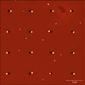
| Integration
|
Integration
59 58
| Integration
Novel Forms of Interconnection and Device Integration for Emerging Multimode, Multicore, Hollow-Core and Multi-Component Optical Fibres
Challenge
To develop novel means of interconnecting emerging new fibre types under development within the Future Photonics Manufacturing Hub to other fibres and/or to other functional components.
Progress
Our research has focused on the development of new fibre optic components, interconnection devices, and characterisation of multi-component soft glass optical fibres.
Firstly, we have investigated the issue of optical interconnection between verticalcavity surface-emitting lasers (VCSELs) and hollow-core fibres (HCFs). Note that direct HCF interconnection to a laser diode or photodiode (i.e. without any short piece of interconnecting solid core fibre) is a very important requirement in order to fully utilise the unique characteristics of HCFs. Many different platforms have been investigated previously in the development of solid core fibre coupled optical devices. During the past year we have focused on two particular HCF interconnection approaches, i.e. direct butt coupling and simple two-lens imaging, for coupling to a VCSEL operating at 850 nm. We observed that butt coupling provides only poor coupling efficiency (~10%) due to the poor mode field diameter mismatch but that a two-lens system can be used to achieve very high coupling efficiency (~96%) with excellent output beam quality. A prototype packaged device was successfully fabricated in-house and in the next period we plan to further explore other semiconductor laser to HCF coupling challenges at other wavelength bands - with particular interest in the interconnection of mid-IR quantum cascade lasers and visible/UV laser diodes to HCFs.

Secondly, using compact micro-optic collimator technology, we have further developed various inline fibre components based on specialty optical fibres. In particular, we have focused on high-power fibre optic components and successfully managed to develop several industrial grade devices (e.g. few mode fibre isolators) operating at >1W with good stability at 1550 nm and supplied these to a commercial partner. In addition, we
Co-Investigator contact: Professor David Richardson, djr@orc.soton.ac.uk
Figure 1: (a) Direct HCF interconnection to a VCSEL and, (b) 3D printed mode scrambler.

have continued our collaboration with NTT in Japan on high spatial density multicore fibre amplifiers (i.e. 6-mode 7-core fibre amplifiers) for ultrahigh spatial density long haul transmission.
We have also worked on low-loss and broadband mode scramblers for mode division multiplexed transmission based on few mode fibres. By simply shortening the length of the long-period fibre grating (LPG), the optical bandwidth can be significantly enhanced. For example, >230 nm bandwidth is predicted in our simulations with a grating length of 0.613 cm. In an experimental demonstration we fabricated a mechanically induced LPG using a commercially available 3-dimensional (3D) printing technique. Wideband operation was confirmed over the C band and a low loss (0.2 dB) and low mode dependent loss (0.1 dB) were achieved.
In addition, we have worked on the characterisation of multi-component soft glass fibres for rare earth doped fibre amplifiers/lasers. In general, soft glasses have poorer glass stability than silica glasses, with low glass transition temperatures and low tensile strengths. Special attention needs to be applied in handling these fibres. Working with the Zepler Institute soft glass fabrication team, we are looking to develop wideband amplifiers using germanotellurite (Ge-Te) glasses which promise broadband emission and improved chemical/mechanical glass stability. In this platform we are working to develop splicing techniques to these fibres and to understand the spectroscopic characteristics of erbium incorporated at high concentrations into the core. Our first target is to develop a compact, seamless C+L band amplifier and our preliminary fibre characterisation results look encouraging in terms of emission and absorption bandwidths. We are also exploring ways to extend the operating bandwidth of silica fibres using multistage designs and optimised inline filtering.
Future Plans
We will continue to focus on the integration aspects of all the emerging fibre types referred to above with a focus on loss reduction, extended wavelength coverage and increasing the range of device functionalities possible.
| Integration
Figure 1a Figure 1b 61 60
Progress on Wideband Optical Amplifiers
Challenge
To exploit the advantages of compound ’soft’ glasses for the development of ultrabroadband optical amplifiers. By widening the amplification bandwidth available to optical communications, we aim to enable a significant increase in transmitted data traffic through the existing optical network infrastructure.
Progress
This year we have focused our activities to the development of optical fibre amplifiers based on non-silica glass hosts. The idea is to exploit the excellent thermo-mechanical properties of glasses developed so far in the hub to produce optical amplifiers with considerably broader amplification bandwidth than the standard ones that use silica as the host material. If this research is successful, these novel fibre amplifiers will be able to support optical communication links with far increased data capacities.

It is well established in the literature that a linear proportionality exists between the refractive index of a rare earth doped glass host and its luminescence bandwidth. ‘Soft’ glasses with a higher refractive index than silica, however, are normally considerably more difficult to draw into useable fibres due to worse mechanical properties and a much higher tendency to crystallisation than silica. Here we exploit the progress made in this project in the previous years in developing robust and crystallisation-free high refractive index glasses. Amongst the various glass host compositions and dopants that we have studied this year, we focus in this report on germanate-tellurite (Ge-Te) glasses doped with erbium, aiming to produce a wideband amplifier cantered around in the C-band of optical communications.
The newly developed Ge-Te glass composition was produced in an ultra-dry glove box furnace, which allows both a dry atmosphere and very low contamination. With an absorption coefficient of <5 dB/m at 3 μm where water absorption peaks, this glass is, to the best of our knowledge, the driest novel soft glass yet developed. Lowering the OH- content in the glass improves its overall spectroscopic characteristics. As can be seen in Figure 1a, the luminescence bandwidth of such a preliminary prototype softglass fibre is very promising, and considerably wider than that of silica. Next, we have optimised the erbium concentration on this type of glass and found that an optimal


Figure 1: (a) comparison between the Erbium emission spectrum of the newly developed Germanate-Tellurite fibre and that of a conventional silica fibre.


Figure 1a
Figure 1b
(b) Fibre fabrication process: from bulk glass billets (cladding: transparent and Er:doped core: pink) to extruded preform and drawn fibre.

existed around 4 mol% (1.76X10²¹ ion/cm3). This concentration was used to prepare the glass for the fibre core. The cladding glass was erbium free, and its composition tailored to provide a refractive index difference that would allow a single mode fibre operation and compatible thermo-mechanical properties with the core glass for fibre drawing (see Figure 1b). Finally, we have recently produced an Er-doped germanate-tellurite fibre from such glasses. Its emission at wavelengths around 1.5 um was measured and it is was found to be twice as large as that of a commercial silica doped fibre. Additional spectroscopic measurements are currently ongoing but these results are already quite promising.
Future Plans
In the near future, we plan to incorporate the newly developed ultra-broadband fibre into an optical amplifier, and to measure its full dynamic performance. Beyond this, we plan to study the incorporation into this very promising host glass of other rare earth elements (Tm3+ Pr3+), as well as of multi active-ion co-dopant schemes such us Er3+/ Tm3+, Er3+/Pr3+ and Er3+/Tm3+/Pr3+. We also plan to study the performance of other ‘soft’ glasses with even higher refractive index, aiming to develop a suite of efficient optical amplifiers covering the full spectral range 1260 – 1675 nm.
| Light Generation and Delivery
| Light Generation and Delivery
Co-Investigator contact: Professor Francesco Poletti frap@orc.soton.ac.uk 63 62
Deputy
Project
Deputy
Public Engagement Leader: Pearl John, University of Southampton
Business Development Manager: Amir Kayani, University of Southampton


Industrial Liaison Manager: Dr John Lincoln

Co-Investigator: Professor Goran Mashanovich, University of Southampton


Research and Relationship PR Officer: Michelle Mitchell, University of Southampton


Principle Investigator and Director: Professor Sir David Payne, University of Southampton

Co-Investigator: Professor Francesco Poletti, University of Southampton
Co-Investigator: Professor Graham Reed, University of Southampton
Co-Investigator: Professor David Richardson, University of Southampton
Co-Investigator: Professor Jayanta Sahu, University of Southampton


Co-Investigator: Dr Natalie Wheeler, University of Southampton

Co-Investigator: Professor Michalis Zervas, University of Southampton
Co-Investigator: Professor Nikolay Zheludev, University of Southampton
| The team
Director and Manager: Professor Gilberto Brambilla, University of Southampton
Co-Investigator: Professor Martin Charlton, University of Southampton
Director: Professor Jon Heffernan, University of Sheffield
Co-Investigator: Professor Dan Hewak, University of Southampton
65 64
Administrator: Liz Gilbride, University of Southampton
With special thanks to: Carbon Trust, Huawei, Honeywell Aerospace, II-VI Photonics, IQE, IS Instruments, Lightpoint Medical, Lumenisity, Merck, Microsoft, NorthLab Photonics, Northrop Grumman, Oclaro, Phoenix Photonics, PragmatIC Printing, QinetiQ, Rockley Photonics, Seagate Ireland, Sestosensor, SPI Lasers, Breakthrough Prize, Defence Science and Technology Laboratory (DSTL), European Office of Aerospace Research & Development, Engineering and Physical Sciences Research Council (EPSRC), European Commission, Horizon 2020, Innovate UK, Royal Academy of Engineering, Royal Society

If you’d like to know more about the Future Photonics Hub, or find out how we can work together, please contact us: +44 (0)23 8059 9536 contact@photonicshubuk.org www.photonicshubuk.org Follow us @PhotonicsHub

