PROTOTYPING AND TESTING
STRATEGIES WITH ORCAD PCB DESIGNER


INTRODUCTION
Prototyping and testing are crucial stages in the development of any electronic product. They ensure that the design meets the required specifications and functions reliably before mass production. OrCAD PCB Designer offers a comprehensive set of tools and features to facilitate prototyping and testing, allowing engineers to iterate quickly and efficiently. In this article, we'll explore prototyping and testing strategies using OrCAD PCB Designer.
1. DESIGN VALIDATION

Before proceeding to prototyping, it's essential to validate the design using simulation tools available in OrCAD PCB Designer. Simulation allows engineers to analyze the behavior of the circuit, verify signal integrity, and assess power distribution. By running simulations early in the design process, potential issues can be identified and addressed before moving to physical prototyping.
2. PCB LAYOUT OPTIMIZATION
Once the design is validated, the next step is to create the PCB layout using OrCAD PCB Designer. During this stage, engineers need to optimize the layout for factors such as signal integrity, thermal management, and manufacturability.
PCB Layout services helps to provide advanced routing and placement tools to achieve optimal layout designs.
3. DESIGN RULE CHECKING (DRC)
Before generating the prototype, it's essential to perform design rule checking (DRC) to ensure that the layout meets the specified constraints and standards.
OrCAD PCB Designer includes built-in DRC features that help identify potential violations such as clearance violations, trace width violations, and solder mask errors. Resolving these issues at this stage can prevent costly errors during manufacturing.
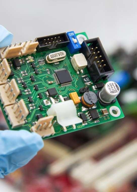
4. PROTOTYPE FABRICATION
Once the PCB layout is finalized, the next step is to fabricate the prototype board. OrCAD PCB Designer supports seamless integration with PCB fabrication services, allowing engineers to generate manufacturing files directly from the design environment. By working closely with fabrication partners, engineers can ensure that the prototype is manufactured to the highest quality standards.
5. COMPONENT ASSEMBLY
After receiving the fabricated PCB, the next step is to assemble the components onto the board. OrCAD PCB Designer provides tools for generating assembly drawings, bill of materials (BOM), and component placement documentation.
Engineers can use this information to facilitate the assembly process and ensure accurate component placement. PCB design services helps in this process.
6. FUNCTIONAL TESTING
Once the prototype board is assembled, it's time to perform functional testing to verify that the circuit operates as intended. OrCAD PCB Designer supports integration with external testing equipment, allowing engineers to perform automated testing and data logging. Functional testing helps identify any design flaws or performance issues that need to be addressed before mass production.
7. DESIGN ITERATION
Based on the results of functional testing, engineers may need to iterate on the design to optimize performance or address any issues uncovered during testing. OrCAD PCB Designer enables rapid design iteration with its intuitive interface and robust design tools. Engineers can quickly implement changes, re-run simulations, and generate updated prototypes as needed.
CONCLUSION
In conclusion, prototyping and testing are essential stages in the development of electronic products, and OrCAD PCB Designer provides the tools and features necessary to streamline these processes. By following the strategies outlined in this document, engineers can efficiently prototype, test, and iterate on their designs, ultimately leading to successful product development.